Continue to Site
Follow along with the video below to see how to install our site as a web app on your home screen.
Note: This feature may not be available in some browsers.
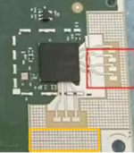
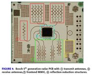
Attachment is another antenna design.
I seems to isolate the antennas.
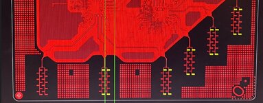
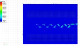
So you have done the test inserting dummy antennas between working antennas.I have done the simulation to insert several fake antennas between working antennas.
The results shows the main lobe gain increases about 1dB,while sidelobe not increasing.
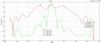
They are possibly electromagnetic bandgap structures. As some have noted, the primary function is likely to prevent radiation/leakage in certain direction, e.g., to isolate the antennas from the rest of the circuitry. They may also be used to enhance radiative performance. If you're lucky, they will do both.I have done the simulation with floating copper.
It seems the floating copper increasing the beamwidth, while increasing the ripple in the band.
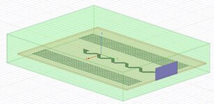
With optimizing on the antenna dimensions, the antenna beamwidth should be increased markably.