Continue to Site

Welcome to EDAboard.com

Welcome to our site! EDAboard.com is an international Electronics Discussion Forum focused on EDA software, circuits, schematics, books, theory, papers, asic, pld, 8051, DSP, Network, RF, Analog Design, PCB, Service Manuals... and a whole lot more! To participate you need to register. Registration is free. Click here to register now.

(ADS Momentm)How to setup port for diode,C,R...?

Status
Not open for further replies.

True koke

Newbie level 6
Joined
Apr 15, 2022
Messages
13
Helped
0
Reputation
0
Reaction score
2
Trophy points
1
Activity points
199
Hi. I am a beginner at ADS Momentum.

I have designed the rectifier using HSMS285C schottky diode.
I also designed layout the rectifier only using TL, but I don't know how to connect the Lumped elements and Diode in ADS circuit and how to setup the port.

My simulation step is like :
1. Sketch the circuit on Layout without any C,Diode,R....
-Because ADS EM simulation does not support Capacitor, R, Diode...
2. I made the Symbol to import to in my circuit.
3. I connected the C,R,Diode with my Symbol.

Please give me advice how to set the port(like Cal. type and connection each other ports to flow the current well..)
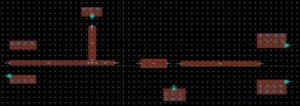
Please refer to the attched image.
layout refr.PNG

Port setup.PNG

Import design.PNG
 

Attachments

  • Layout.PNG
    Layout.PNG
    17.4 KB · Views: 197
I'm afraid I caused confusion with my post on grouping pins in the previous thread.

There is a mistake with the diode (P4/P5/P7).

By grouping pins P4 and P5 into one port, you enfore a two terminal device: the only way of P4 current is to leave at P5 then. But your device has three pins, not two, so you need to ungroup the pins at the diode and have three independent ports.

When using EM results in schematic, grouping of pins to ports is not required here. The wiring of EMmodel at schematic level is sufficient, there is no need to group the pins into one port with explicit ground. You can leave all pins with global ground (substrate backside) and make connections at schematic level.

~~

Calibration: TML is ok for your input port, but only works if both pins are located on the same plane at the polygon boundary. It seems that P12 is located inside the polygon, then TML will not work, and it will switch calibration to "None" behind the scenes.

Using calibration "none" for the other elements is ok here, to keep it simple. The layout looks not finalized (detailed) anyway, and port cal has very little influence at your frequency of interest. Details like proper component size and footprint have much more effect than port cal.

Best regards
Volker (Keysight Certified Expert EDA)
 
Last edited:
I'm afraid I caused confusion with my post on grouping pins in the previous thread.

There is a mistake with the diode (P4/P5/P7).

By grouping pins P4 and P5 into one port, you enfore a two terminal device: the only way of P4 current is to leave at P5 then. But your device has three pins, not two, so you need to ungroup the pins at the diode and have three independent ports.

When using EM results in schematic, grouping of pins to ports is not required here. The wiring of EMmodel at schematic level is sufficient, there is no need to group the pins into one port with explicit ground. You can leave all pins with global ground (substrate backside) and make connections at schematic level.

~~

Calibration: TML is ok for your input port, but only works if both pins are located on the same plane at the polygon boundary. It seems that P12 is located inside the polygon, then TML will not work, and it will switch calibration to "None" behind the scenes.

Using calibration "none" for the other elements is ok here, to keep it simple. The layout looks not finalized (detailed) anyway, and port cal has very little influence at your frequency of interest. Details like proper component size and footprint have much more effect than port cal.

Best regards
Volker (Keysight Certified Expert EDA)

Thanks again, :)

But I'm confusing how to set the Port calibration and +,- terminal...
You said that "When using EM results in schematic, grouping of pins to ports is not required here. The wiring of EMmodel at schematic level is sufficient, there is no need to group the pins into one port with explicit ground."

But according to the below link, it is necessary to group the Pin to flow current well between the separated TLs.
So,,I'm very confusing...


The example from my website that you linked shows importance of port ground reference. If all your ports share the same global ground you are "safe" to use that in layout look-alike.

Grouping pins to ports has an effect on the "raw" S-parameters from EM simulation. If you do NOT group them, you have maximum degrees of freedom in wiring the EM Model.

Believe me that you should not group pins to ports for the case show above. The required connections are made at schematic level, so don't worry!
Thank you so much.
I modified as you advice, and then I checked the result.
But there is a strange thing. The efficiency is very defferent depending on where Vout net and R.
The first image's efficiency is about 100~120%.
And second image's efficiency is about 20~30%.
The equotion to calculate efficiency I have used : efficiency = real(Vout[::,0])*real(Vout[::,0])/R/dbmtow(Pin)*100

Can I know What is correct?
first.PNG

second.PNG
 

Have you changed the EM model back to ports with global ground?

Create a test schematic with the look-alike and two ports (ADS element: Term). One port is conected to P8, the other port is connected to P9. Show the impedance into each of these ports in Smith chart, for wideband sweep from DC to 3 GHz. Both should be close to short circuit.
Dear volker,

When I checked efficiency of rectifier in 2D circuit, the efficiency is about 75%..
But when I import the EM data with symbol to circuit, the efficiency is about 25%...
What is wrong..?
I did this simulation about 1 month.. but I don't know what the problem is.

At first, I thought the VIA was a problem, so I deleted the VIA and connected it to the common ground, but the results were the same. From this, I think I know that Via is not the problem, but my layout or setting.
1.PNG
2.PNG
3.PNG
 
You should test things step by step. Did you do the tests that I described above?

You need to define EM frequency range starting at DC, did you do that?

You can replace parts of the schematic by EM Model step by step, to see what is critical. Troubleshooting your simulation in a systematic way is part of the engineering job. Test your EM results if they make sense at DC also.

I changed the frequency range from 0 to 4GHz.
That's a surprising result. I just changed the frequency range, but the efficiency went back up to 64 percent!!

Could you please the reason?

In the case of rectifiers, I know that the goal is to obtain DC, but in the result window, it seems that the efficiency is simply low at 2.45 GHz.

Now that I've used the common ground to see how efficient it is, I just need to make some vias and test it.
I have an additional question, is there any difference between using C_Pad with port and just connecting ports without Pad to the space where capacitors will be used?
 

I changed the frequency range from 0 to 4GHz.
That's a surprising result. I just changed the frequency range, but the efficiency went back up to 64 percent!!

This is no surprise, because your schematic simulation covers 2.4 GHz and DC. If you EM simulate at 2.4 Ghz only, there is no information on DC behaviour in your EM Model, and ADS will use extrapolation. But extrapolation from 2.4 GHz down to DC is very inaccurate here.


I have an additional question, is there any difference between using C_Pad with port and just connecting ports without Pad to the space where capacitors will be used?

I don't understand your question. Momentum simulates the layout, no more and no less. If you want to include the effect of component pads (more area = more capacitance to ground) the pads must be included in layout. Using C_Pad is one possible way to include them.

It is always a good idea to EM-simulate the layout that you will build in hardware. Your layout has pads, so you better simulate them.
 

This is no surprise, because your schematic simulation covers 2.4 GHz and DC. If you EM simulate at 2.4 Ghz only, there is no information on DC behaviour in your EM Model, and ADS will use extrapolation. But extrapolation from 2.4 GHz down to DC is very inaccurate here.


I don't understand your question. Momentum simulates the layout, no more and no less. If you want to include the effect of component pads (more area = more capacitance to ground) the pads must be included in layout. Using C_Pad is one possible way to include them.

It is always a good idea to EM-simulate the layout that you will build in hardware. Your layout has pads, so you better simulate them.
Thank you for reply.

I mean, I wonder if the accuracy can be improved by drawing a Pad on a layout with a capacitor and a resistor and simulating it.

As you know in my layout, I only drawn the pin for connecting C,R,Diode in circuit.
I didn't drawn the Pad in layout because they doesn't support C pad like below image.
support no.PNG


Thanks in advance.
 

Of course, more accurate modelling of the actual layout will improve accuracy. I haven't used C_Pad in my Momentum models, if it doesn't support automatic partitioning you might need to add ports yourself.

But this forum cannot replace Momentum tutorial and training, sorry for that. There are many good youtube tutorials by Anurag: https://www.youtube.com/channel/UCuo4ZHW4J5k0EmuyKG8kYEA
Thanks for your kind reply.

I finally did rectifier EMsimulation well and my rectifier has more than 60% efficiency.
The range above 50% efficiency is approximately 500 MHz.

Thanks again. I think the problem was solved.
And also I'll refer to the Youtube link for doing tutorial.
 

Status
Not open for further replies.

Part and Inventory Search

Welcome to EDABoard.com

Sponsor

Back
Top