Continue to Site

Welcome to EDAboard.com

Welcome to our site! EDAboard.com is an international Electronics Discussion Forum focused on EDA software, circuits, schematics, books, theory, papers, asic, pld, 8051, DSP, Network, RF, Analog Design, PCB, Service Manuals... and a whole lot more! To participate you need to register. Registration is free. Click here to register now.

Forward bias PNP base emitter diode with AC coupled input

Status
Not open for further replies.

tortoise

Newbie
Joined
Feb 14, 2020
Messages
4
Helped
0
Reputation
0
Reaction score
0
Trophy points
1
Activity points
48
Hi, I'd really appreciate some help with understanding the following level converter which is meant to convert the input signal (via C3) into the base of the PNP (Q4) to 3.3V/0V at the collector of Q5. The emitter of the PNP is at 36V and its base is driven with a signal that's meant to vary between 36V and 24V @ 2.5khz but sometimes only dips to 28-30V. My understanding is that the PNP should turn on every time the input dips even 1-2V below the emitter.
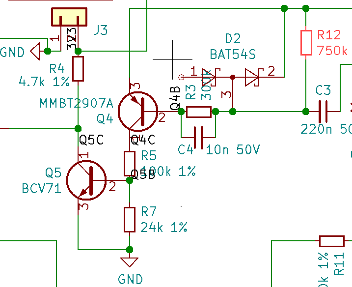
recv.png


I've tried a ltspice simulation and it seems to work as expected but in my prototype Q4 refuses to turn on. The components seem to be ok/undamaged. This is part of a larger circuit and everything else works as expected. Can the base of the PNP ever get pulled low wrt the emitter in this circuit? What else could be wrong here? Thanks.
 

Hi,

The usual signal flow on a schematic should be from left to right.

I don't know what voltage is on the upper node of R12.
But - just guessing - for proper biasing I'd expect R12 to go to GND....

Klaus
 
I think the diodes are blowing because 36V exceeds their max. rating.
There might be a unwanted voltage drop ( less positive) at the anode of the diodes.
Check this node with an oscilloscope and see what happens at that node.If the event is according to my explanation, change the configuration.
Simulators do generally not show these kind of phenomena.
 

PNP transistors are shut off when bias sees the same voltage as the emitter (upper leg). This appears to be the usual condition for Q4 (as you state, receiving 36V through R3 R12, about 1 megohm).

In order to turn on Q4 bias, net voltage needs to pulled down sufficiently (a volt or two) by signal coming through C3. You state your signal has DC level a few volts below the bias pin, with AC swing of several volts. In addition I think this also needs to come through impedance much less than a megohm, in order to overcome 36V coming through 1 megohm. It also may help if you increase value of C3 & C4.
 
I confirm that circuits like this can be well examined with a circuit simulator. Some points should be however considered:
- SPICE is modelling with typical component parameters, e.g. transistor current gain can vary over a larer range. If you circuit is sensitive against current gain variations, you should also test with marginal (minimal, maximal) current gain.
- SPICE models usually don't include maximum ratings and self-heating of components .

A possible way is to compare simulation with measured waveforms and find out what's different.
 

    tortoise

    Points: 2
    Helpful Answer Positive Rating
Hi,

The usual signal flow on a schematic should be from left to right.

I don't know what voltage is on the upper node of R12.
But - just guessing - for proper biasing I'd expect R12 to go to GND....

Klaus

Schematic onvention of signal flow noted. Thanks.

Upper node of R12 is at same voltage as emitter (36V). I'll try grounding bottom node of R12 (maybe via another resistor 100k?). Thanks.
 

Upper node of R12 is at same voltage as emitter (36V). I'll try grounding bottom node of R12 (maybe via another resistor 100k?).
This will turn Q1 permanently on - no good idea.
 

    tortoise

    Points: 2
    Helpful Answer Positive Rating
I confirm that circuits like this can be well examined with a circuit simulator. Some points should be however considered:
- SPICE is modelling with typical component parameters, e.g. transistor current gain can vary over a larer range. If you circuit is sensitive against current gain variations, you should also test with marginal (minimal, maximal) current gain.
- SPICE models usually don't include maximum ratings and self-heating of components .

A possible way is to compare simulation with measured waveforms and find out what's different.

Thanks for the input. The input into the base of Q4 is 'generally' consistent with the spice simulation - I'll take a closer look and report back with any new differences I spot.
 

This will turn Q1 permanently on - no good idea.

Did this just to check the component (Q4). I can't get it to turn on with a 100k resistor from the bottom of R12 to ground. Tried different pieces/boards but can't currently test it without R12 as I only have assembled boards. I hope it's not an error with the component - It's definitely a PNP as the diodes point into the base (tested using multimeter). I don't see anything in the datasheet that should prevent it from turning on with this setup.
 

Attachments

  • MMBT2907A_pnp.pdf
    245.3 KB · Views: 80

I presume the problem can be narrowed down by measuring all node voltages with a multimeter.

Q4C base node can be e.g. open or shorted to emitter, R3 can have some or no voltage drop, D2 terminals may be flipped, preventing Q4C turn-on etc.
 

Status
Not open for further replies.

Similar threads

Part and Inventory Search

Welcome to EDABoard.com

Sponsor

Back
Top