Continue to Site

Welcome to EDAboard.com

Welcome to our site! EDAboard.com is an international Electronics Discussion Forum focused on EDA software, circuits, schematics, books, theory, papers, asic, pld, 8051, DSP, Network, RF, Analog Design, PCB, Service Manuals... and a whole lot more! To participate you need to register. Registration is free. Click here to register now.

gm/Id Method in designing Op-Amps - How do you choose the gm/Id value?

Status
Not open for further replies.

esdeath_123

Junior Member level 3
Joined
Sep 30, 2018
Messages
25
Helped
0
Reputation
0
Reaction score
0
Trophy points
1
Activity points
236
I'm trying to design a two stage Miller Op-Amp using gm/Id method. Figure 1 OTA.png
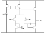
Starting from the second stage, from a given set of specifications, I found out that the gm and Id of the second stage can be computed. My question is, what if the computed gm/Id is out of bounds? From simulations, I was able to see that gm/Id has a max value of around 20-30 depending on the transistor. Do I adjust the current and/or the gm to set it within range? But this would change the overall GBWP and/or the Slew rate of the op-amp. And if I should change the gm/Id, what value should I set it to?

Also, some of my teachers say that from gm/Id, one can estimate vdsat. They said that 20 is around 100mV vdsat and 15 is around 200mV vdsat, always, IIRC. How is this done? Doesn't gm/Id and vdsat change depending on the transistor?

Finally, how do you set a gm/Id value? What I know is that it is also related to inversion regions (weak, strong, moderate) and that operation in weak inversion results to high gain, low bandwidth, high gm/Id and larger devices while strong inversion is the opposite and moderate is a balance of the two. Is this correct? What are other factors in choosing gm/Id?
 

If you are out of bounds, so change gm/Id to be between bounds as far as you meet specification.

VDSsat and other parameters are computed by simulator e.g. Cadence. You can make them visible on schematic. :)

So far I haven't seen a person who used gm/Id methodology in a professional environment in a general circuit design (comparators, opams in single-to-hundreds MHz bandwidth range, bandgaps so on). More persons rather look at matching and Monte Carlo simulations. Based on that, W/L dimensions are set.
 

gm/Id is a good method and quite helpful when used in designing circuits. Question is, esdeath_123, why do you want to use it?
From your post I understood that you want to choose either current to get some gm/I or choose gm, to achieve the same. In my view this is not the purpose of the gm/Id methodology. Used for design, gm/Id is your design variable, not gm or I separately.
gm/Id can specify your gm/Cgg, which is speed of the circuit, it can be used to determine gm/gds, which is the gain of the circuit, or it can be used to determine I/W, which is the biasing of your circuit.

Given technology transistors you can't go beyond the limits for gm/Id (from about 4 to about 25 or 30). Beyond these limits your transistors are not functional, so no point of even thinking about values outside this range. Low gm/Id corresponds to strong inversion i.e. lots of current for given gm. High gm/Id corresponds to weak inversion - lots of gm for given current. Also, gm/Id is a proxy for Vov or the saturation voltage. Vov=2/(gm/Id), so yes, gm/Id=20 corresponds to Vov=100mV, but Vov=200mV is gm/Id=10, which is a pretty often used value.
Ways to design with gm/Id as your primary variable are many and versatile, so it is not possible to give a single recipe. For your amplifier for example, you can choose the GBW you target which is gm1/Cc. You could pic Cc based on noise and define gm1 for that GBW. Or maybe you could determine what Vov of your input diff pair you need based on few things but say based on input common-mode range. Then you could pick the tail current based on power consumption considerations. Or other variations. Conversely, if you know what gain you need from the 1st stage based on L and the intrinsic gain of the transistors gm1/gds you could pick gm/Id.
In any case, when you have the gm/Id, you could find I/W and thus decide on the W of the transistor.
For all this, though, you need to have characterized your transistors for use with the gm/Id. That means you need to have extracted curves for I/W vs. gm/id; gm/Cgg vs. gm/Id; gm/gds vs. gm/Id. This is a normalized design space where nothing depends on W of the transistors and depends very weakly on Vds. In fact W is the outcome of the design procedure. These curves depend on L, though, so they need to be extracted for different L.
Bottom line, if you want to use gm/Id methodology, you need to do some reading first.
 
Last edited:
@sutapanaki
It looks it's a task at esdeath_123's university.
 

gm/Id is a good method and quite helpful when used in designing circuits. Question is, esdeath_123, why do you want to use it?
From your post I understood that you want to choose either current to get some gm/I or choose gm, to achieve the same. In my view this is not the purpose of the gm/Id methodology. Used for design, gm/Id is your design variable, not gm or I separately.
gm/Id can specify your gm/Cgg, which is speed of the circuit, it can be used to determine gm/gds, which is the gain of the circuit, or it can be used to determine I/W, which is the biasing of your circuit.

Given technology transistors you can't go beyond the limits for gm/Id (from about 4 to about 25 or 30). Beyond these limits your transistors are not functional, so no point of even thinking about values outside this range. Low gm/Id corresponds to strong inversion i.e. lots of current for given gm. High gm/Id corresponds to weak inversion - lots of gm for given current. Also, gm/Id is a proxy for Vov or the saturation voltage. Vov=2/(gm/Id), so yes, gm/Id=20 corresponds to Vov=100mV, but Vov=200mV is gm/Id=10, which is a pretty often used value.
Ways to design with gm/Id as your primary variable are many and versatile, so it is not possible to give a single recipe. For your amplifier for example, you can choose the GBW you target which is gm1/Cc. You could pic Cc based on noise and define gm1 for that GBW. Or maybe you could determine what Vov of your input diff pair you need based on few things but say based on input common-mode range. Then you could pick the tail current based on power consumption considerations. Or other variations. Conversely, if you know what gain you need from the 1st stage based on L and the intrinsic gain of the transistors gm1/gds you could pick gm/Id.
In any case, when you have the gm/Id, you could find I/W and thus decide on the W of the transistor.
For all this, though, you need to have characterized your transistors for use with the gm/Id. That means you need to have extracted curves for I/W vs. gm/id; gm/Cgg vs. gm/Id; gm/gds vs. gm/Id. This is a normalized design space where nothing depends on W of the transistors and depends very weakly on Vds. In fact W is the outcome of the design procedure. These curves depend on L, though, so they need to be extracted for different L.
Bottom line, if you want to use gm/Id methodology, you need to do some reading first.

Thanks for the reply! I do know how to get the curves needed and how to eventually get the L and W for each transistor. What I'm only having trouble is deciding which gm/Id value to use. I do know that at higher gm/Id, low current and high gm is present and vice versa. However, is wanting low current or high transconductance enough of a reason to choose higher gm/Id and vice versa? For example, why would I want a gm/Id of 20, which results to a vdsat of 100mV or why would I want gm/Id of 10, which as you say is a pretty often used value? And why is this often used? I have seen in forums that it is usually preferred to operate in 100mV vdsat but they fail to mention as to why it is preferred...Can you clarify? Still a bit confused...
 

I do know that at higher gm/Id, low current and high gm is present and vice versa.

Be careful of this statement. gm per unit Id is higher if you keep decreasing Vgs, but it comes at a cost of lower gm. In that case, you will need to size up your devices to get more gm and this will impact your poles due to device capacitances.

Also, your choice of vdsat depends on your voltage headroom available to you and your Vdd. In a real amplifier, you need to allow some output swing and this will set the limits on your vdsat.
Refer to "Analog Design Essentials" by Willy Sansen where he really works out how to design a Miller compensated op-amps. He has nice neat little formulas.
 
The other name for the gm/Id is current efficiency. In other words, how much current you have to invest to get a certain gm. The best current efficiency you get in weak inversion because there gm/Id is highest and you get largest gm for a given current invested. But as we all know, weak inversion is not good for speed, that is for highest current efficiency you pay with high Cgg, which means gm/Cgg is small.
Traditionally, Vov=200mV has been like a rule of thumb, which is gm/Id=10. With modern day technologies - 40nm, 28nm, 16nm... it is actually too much and people work with Vov=100mV or 150mV, or whatever is needed.

Unless you try to get a specific value for Vov, you don't usually just choose gm/Id. It comes as a result of other considerations, maybe from speed, maybe from noise, or maybe from something else.

Also, designing a circuit, you may need to go through couple of iteration before the result converges.

You probably already know this, but in case you don't there are some examples in this link

**broken link removed**


Or here


https://www.ece.tamu.edu/~spalermo/ecen474/lecture07_ee474_gmid.pdf
 
Last edited:
The other name for the gm/Id is current efficiency. In other words, how much current you have to invest to get a certain gm. The best current efficiency you get in weak inversion because there gm/Id is highest and you get largest gm for a given current invested. But as we all know, weak inversion is not good for speed, that is for highest current efficiency you pay with high Cgg, which means gm/Cgg is small.
Traditionally, Vov=200mV has been like a rule of thumb, which is gm/Id=10. With modern day technologies - 40nm, 28nm, 16nm... it is actually too much and people work with Vov=100mV or 150mV, or whatever is needed.

Unless you try to get a specific value for Vov, you don't usually just choose gm/Id. It comes as a result of other considerations, maybe from speed, maybe from noise, or maybe from something else.

Also, designing a circuit, you may need to go through couple of iteration before the result converges.

You probably already know this, but in case you don't there are some examples in this link

**broken link removed**


Or here


https://www.ece.tamu.edu/~spalermo/ecen474/lecture07_ee474_gmid.pdf

Thank you for the reply! The references you provided were helpful, especially the first one.
 

A question, btw. Do you need to set the gm/Id of all transistors in an op-amp to be equal? Or will this also depend?
 

Obviously you need to set it for the symmetric transistors - for example the input devices of the diff pair or the load devices in the diff pair.
 

Obviously you need to set it for the symmetric transistors - for example the input devices of the diff pair or the load devices in the diff pair.

That I know much :) What I'm asking is if it's alright to set all the transistors in an op amp to be equal? Or is equal gm/Id possible only for symmetric transistors?
 

What I'm asking is if it's alright to set all the transistors in an op amp to be equal? Or is equal gm/Id possible only for symmetric transistors?
You (ideally) should not care about the gm of your load pair or your tail current source. You want a high output impedance of those devices (to maximize gain) as well as a low overdrive (to maximize swing). But at the same time you don't want the devices to be too large else the parasitic capacitance because of the devices will cause you a degradation in phase margin.
 
That I know much :) What I'm asking is if it's alright to set all the transistors in an op amp to be equal? Or is equal gm/Id possible only for symmetric transistors?

Given the different considerations that lead to the choice or result into values for gm/Id, no, there is no such guarantee that devices will have same gm/Id. They might in certain cases, but it is not a rule.
 
That I know much :) What I'm asking is if it's alright to set all the transistors in an op amp to be equal? Or is equal gm/Id possible only for symmetric transistors?

As answers above, it is rare that all your transistors e.g. in opamp are equal. Transistors may serve different purposes: differential pair, active load, cascoding, current mirror etc. Hence, their dimensions may vary.
 

As answers above, it is rare that all your transistors e.g. in opamp are equal. Transistors may serve different purposes: differential pair, active load, cascoding, current mirror etc. Hence, their dimensions may vary.

Sorry for the confusion. What I meant was same gm/Id, not same dimensions.
 

Status
Not open for further replies.

Similar threads

Part and Inventory Search

Welcome to EDABoard.com

Sponsor

Back
Top