Continue to Site

Welcome to EDAboard.com

Welcome to our site! EDAboard.com is an international Electronics Discussion Forum focused on EDA software, circuits, schematics, books, theory, papers, asic, pld, 8051, DSP, Network, RF, Analog Design, PCB, Service Manuals... and a whole lot more! To participate you need to register. Registration is free. Click here to register now.

LTC4020 Battery Charger not charging full current

Status
Not open for further replies.

ben5243

Member level 3
Joined
Feb 26, 2019
Messages
55
Helped
3
Reputation
6
Reaction score
3
Trophy points
8
Activity points
849
Hi all, I've read through the other LTC4020 threads on here but couldn't find my problem.

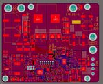
I've prototyped a LTC4020 buck boost charger for a Li-ion battery meant to charge 7-cell at 10A maximum.
Input Voltage: 19-29V (24V nominal)
V_float (CV): 29.375V
Vmax: 32.31V
Vmin: 24.97V

The RNG_SS pin will eventually be servo'd by a MCU to limit the current per the datasheet but right now the jumper resistor is unpopulated and the RNG_SS pin just has a 1uF capacitor to GND for slow start so the charger is independently operating.

The Vout voltage is correct (32.31V with no battery) so the buck-boost converter appears to be working, however it is only charging my battery (at 25V right now) at around 0.7A. Rcs = 0.005Ohm so charging limit is 10A

When the battery is connected, the Vout from the buck boost converter drops to the battery voltage (about 25V right now). There is about 11mV drop over the powerpath FET so it does not appear the controller is limiting the charge current here.

Rsensea = Rsenseb = 0.003Ohm so the Inductor maximum current is set to 16.7A (inductor is rated for 24A with saturation current of 21A). The benchtop power supply is showing a current draw of 1.0A at 24V and the FETs are cool to touch and the inductor is warm, but barely above room temperature. The inductor is


Okay here is the weird stuff:
1.) The RNG_SS pin (for slow start) shows in the datasheet that it supplies 50uA to a capacitor and has an effective range from 0 to 1V. I measure this pin and the capacitor is charged to 3.0V. Is this normal?

2.) I've left the I_Limit pin floating to match all 3 application examples in the datasheet and I'm unsure I can safely probe the leadless package at the pin to check the voltage here - is it important to connect a slow start capacitor here or could this cause a false I_Limit setting?

I would greatly appreciate any suggestions for what to test or check next in my circuit as I am out of ideas. I have scope'd all 4 gate outputs and they all appear to output PWM signals but I'm unsure if they are correct as there's no example waveforms in the datasheet.

I can post some scope captures of specific pins if someone could let me know which are useful. I did not want to post 100 captures if they are all unhelpful.

- - - Updated - - -

Okay I was able to probe I_limit and it is also 3.0V, same as RNG_SS. I don't think this is normal, should I try replacing the IC?
 

Hi,

It's a power switching applications.
Thus the PCB layout is very important.

Can we see your schematic and your PCB layout?

Klaus
 

Hi,
I've attached the layout and schematic. The lower left is local power supplies and MCU. The LT4020 is on the lower right.

In the schematic, R34 is not populated (will connect the RNG_SS pin to 0-1V signal)
I've also cut the trace to PVIN and connected PVIN to INTVCC and the 5V supply instead of using the internal INTVCC regulator (same as described in datasheet). PVIN and INTVCC are stable at 4.94V
fig9.jpg
 

Attachments

  • layout.jpg
    layout.jpg
    255 KB · Views: 228
  • Battery Charger Sh01.pdf
    461.3 KB · Views: 200
Hi,

I just had a quick view through your schematic.

Where are the GNDs connected? GND_C, PGND, SGND

Klaus
 

Thanks for looking.
GND_C is from a common mode choke for the local power supplies. Top left of the attached page. 5V and GND_C are the rails for the MCU.
I guess now that I modified the board to connect PVIN to the 5V supply, the return path is not through the same choke. I will try going back to using the INTVCC internal supply.

PGND and SGND I had to connect on the PCB with solder between copper pours (I forgot to add a net-tie). It connects to PGND at the negative terminal of the VOUT bypass capacitor, as suggested by the datasheet.

Also, I did replace the LTC4020 with a new one and the behavior is identical. RNG_SS is still 3.0V to both PGND and SGND

- - - Updated - - -

I've reconnected the board as drawn in the schematic (using internal INTVCC) and there is no change. Charge current is still between 0.7 and 0.8A

Is FET shoot-through a possibility? Would that result in very slow charge current?
None of the FETs get warm. Are there some signals I can capture on the scope that would help troubleshoot? I'm not very familiar with buck-boost converters so I don't know exactly what to look for.
 

Attachments

  • Battery Charger Sh03.pdf
    209 KB · Views: 160

Hi,

R6 is 3mOhms and has to senses short current peaks.
Thus it needs careful PCB layout and kelvin wiring to the LTC4020.
I can't see how this is done in your layout.
Can you highlight the wiring?

Klaus
 
Klaus,

Thanks very much for the suggestion. I did not Kelvin connect R5 and R6 (embarrassing) for Rsensea and Rsenseb. I did for the battery charging resistor but forgot on those two.
The traces are connected to vias near the resistor pads on the copper pours and are not routed together back to the LTC4020. The loop area is not big but it could be much better.
I will do some testing with the oscilloscope to see if there is a difference in waveform at the chip compared to the top pads on the resistor and try to modify the board if there is.

- - - Updated - - -

Update:
I think I have found something interesting. The voltage measurement on the high side Rsense resistor (R5 for me) shows wildly high current spikes. Here is a scope capture across R5 (touching the top bands of the chip resistor, not the solder on both sides)

DSC_0705.JPG
The DC/DC converter has no load during this capture.
This is voltage over a 3mOhm resistor so each division is 66A

Zooming in on one of those "spikes" shows many individual transients:
DSC_0704.JPG

Zooming in close on the first two "spikes" in the above capture looks like this:
DSC_0703.JPG
Over the 3mOhm resistor, this spike is indicating a current of 0.616/0.003 = 205A

This must be shoot-through on the FETs, right?

When the DC/DC converter is loaded, the "zoomed out" view looks like this:
DSC_0706.JPG
 

Hi,

What exact brand and type are these resistors?

Klaus
 

R5 and R6 are Panasonic ERJ series. 1% tolerance, 1W power rating, 2512 SMD package
https://www.digikey.com/product-det...ic-components/ERJ-M1WSF3M0U/P3.0MCT-ND/300469

They are marked "3MO" on the chip but I cannot verify what the marking should be from the datasheet - there is no marking code. It does not
My multimeter will only measure to 0.1Ohm
I could remove one from the board and set up a test circuit to verify resistance... but I have never had digikey send the wrong part.
 

New information:
As an experiment, I've removed the parallel FETs. I originally left pads for 2 FETs per switch (same as the Demo board DC2134A) as an option to increase switching capacity if heat was an issue but I populated both in my prototype.

The board now charges the battery at 2.5A so that is progress! I think it is certainly a switching shoot-through problem. Removing the parallel FETs should have cut the gate capacitance in half.
I would like to use the SiR664DP FETs that are used in the demo board, but could only find SiR688DP FETs. Slightly higher gate capacitance and slower switching times which is probably part of my problem.

I've been trying to read up on shoot-through caused by di/dt transients and how to diagnose/prevent it but I'm struggling to understand. Power electronics is not my strong area. Does anyone have a crash course on half-bridge shoot through protection? I'd like to try adding some "snubber" circuits but I don't know where to start.

It also does not seem there is a way to adjust the deadtime between switching on the LTC4020, which is only 75ns.

Thanks
 

Anyone?

Are the SiR664DP FETs really that much better than the SiR688DP FETs? The demo board has space for 8 of them with no snubber cicuits, gate resistors, diodes, or bootstrap resistors to mitigate shoot-through.

If I redesign this board on a 4 or 6 layer stackup, what's the best way to reduce any coupling/parasitic inductance on the gate traces? It seems most FET driver ICs prefer to be positioned as close to the FETs as possible (like opposite side of the board) and have short traces, but because of all the sense resistors and battery charging sensing, the LTC4020 shouldn't be mounted near the switching and high current elements of the board, right?

L1 - top current paths
L2 - signal ground plane covering the entire board?
L3 - gate drive traces?
L4 - Rsense current feedback traces?
L5 - signal ground plane covering entire board?
L6 - bottom current paths/heat dissipation

Is that the proper stackup to avoid coupling and shoot-through? Where do L2 and L5 connect to the outer layers and each other?

I'm still quite confused about where to connect the SGND and PGND separated planes. In the datasheet it says not to route current sense traces across differing ground paths but this is exactly what they've done on the demo board. It also says to connect the SGND to the PGND at the negative terminal of the Vout capacitors but in the demo board they have done it completely different.
 

It sounds as though your project uses synchronous switching rather than a diode. Since a battery is the load your mosfet needs to turn off at exactly the right moment so current flow stops, or doesn't flow in the wrong direction. I think a freewheeling diode during off-time would make it easier to diagnose issues.

Simulation showing expected waveforms. Your schematic has an inductor 22uH. My (theoretical) simulation arrives at 50 kHz for a suitable switching frequency, if you want average Ampere level = 10A.

buck-boost clock-driven 24VDC 50kHz 15A to 25v bat'y.png

Behavior of the circuit is easier to grasp by putting an NPN as the switch at the low side. Notice current flows upward through the upside-down battery.
 

You are pretty close but more info is needed to track down the cause - posting soft start waveforms will tell if it works properly up until some other control takes over...

Could you tell me what is the most useful waveforms to look at? I have a 2 channel scope with single reference so I can only look at 2 signals simultaneously with the same reference.


Update - Linear Tech support has finally responded to me in regard to questions on their LTC4020 datasheet (after 2 weeks) and included their proprietary design spreadsheet for the LTC4020. It's password protected so I cannot see how they calculate their values however.
I've updated it with all my specifications and their suggested choke is 0.6uH also, however that results in huge inductor currents (50A Ipeak).
If I put 5.6uH into the spreadsheet, it shows the IL choke current range from 18.5A (at Vin=22V) to 15.7A (at Vin=26V). My RsenseA/B sense resistors are 3mR for 16.6A Iavg limit.
spreadsheet.jpg

I guess I need to increase the Iavg limit?

It brings me back to these equations from the datasheet:
IL.jpg

Using 12A output (same as spreadsheet), I do not get the same values the spreadsheet gets at Vin=22V
IL ~ 12A * (29.2/22)
...
IL ~ 15.9A So where does the 18.3A come from? Safety factor?

The spreadsheet also says Ipeak with a 5.6uH choke is 23.5 A (at Vin=22V)

My choke (for right now) is 5.6uH, Irated= 19A, Isat = 33A.
Where would I find a better suited inductor that won't exceed maybe +20C rise under these conditions? It can be toroidal wound, space isn't a big issue. Digikey seems to only have SMD inductors.
 

Consider interleaving two or more converters:

twin interleaved buck-boost 100kHz charge 27v bat 19A peaks (ana-swi).png

By configuring your control IC it should be feasible to change duty cycle, to overlap On-times, overlap Off-times, taper charging Amperes, etc.

To keep this demo simple as possible I set a 50 percent alternating duty cycle.
 

Status
Not open for further replies.

Similar threads

Part and Inventory Search

Welcome to EDABoard.com

Sponsor

Back
Top