Continue to Site

Welcome to EDAboard.com

Welcome to our site! EDAboard.com is an international Electronics Discussion Forum focused on EDA software, circuits, schematics, books, theory, papers, asic, pld, 8051, DSP, Network, RF, Analog Design, PCB, Service Manuals... and a whole lot more! To participate you need to register. Registration is free. Click here to register now.

Opamp integrator practical circuit

Status
Not open for further replies.

promach

Advanced Member level 4
Joined
Feb 22, 2016
Messages
1,199
Helped
2
Reputation
4
Reaction score
5
Trophy points
1,318
Activity points
11,636
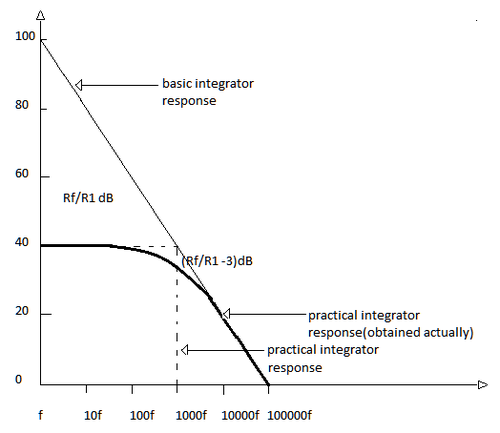
For https://en.wikipedia.org/wiki/Op_amp_integrator#Practical_circuit , why "To negate the effect of the input bias current, it is necessary to set: Ron = R1 || Rf || RL " ? What is Ron ? Is it similar to Rom ?

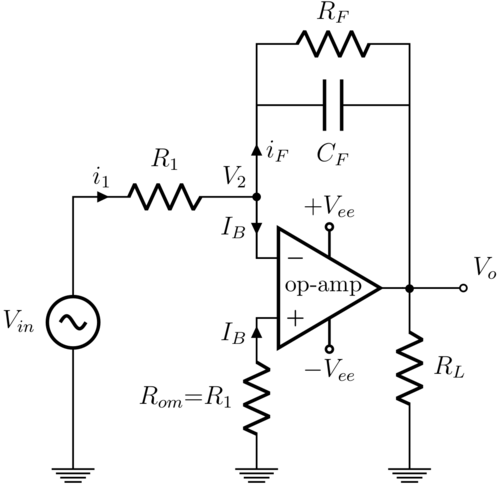
Why is Rf inside that expression when Rf does not share the same gnd node as RL and R1 ?

500px-Practical_integrator.png
 

What is Ron?
A typo, obviously it means Rom.

The compensation resistor is only meaningful for OPs with Ibias > Ioffset, only classical OPs with BJT input stage and no input current compensation. In other words, inappropriate for most modern OPs.

Why is Rf inside that expression when Rf does not share the same gnd node as RL and R1?
Not a question of ground connection. Consider zero input voltage and wanted zero output voltage. You'll see that Ib output effect is exactly cancelled for the given resistor dimenioning.
 
A typo, obviously it means Rom.

The compensation resistor is only meaningful for OPs with Ibias > Ioffset, only classical OPs with BJT input stage and no input current compensation. In other words, inappropriate for most modern OPs.


Not a question of ground connection. Consider zero input voltage and wanted zero output voltage. You'll see that Ib output effect is exactly cancelled for the given resistor dimenioning.

I've read a large number of opamp datasheets in recent times and haven't noted very many where Ibias wasn't speced higher than Ioffset.

For example this is a CMOS "e-trim" (trimmed digitally after packaging) and Ibias is 5X Ioffset:
https://www.ti.com/lit/ds/symlink/opa727.pdf

I imagine this is an example of what you're talking about however the max Ibias is still larger than Ioffset over full temp. Would you argue that matching input impedances in this case isn't worth it?
https://www.ti.com/lit/ds/symlink/opa140.pdf


As to the OP's question look up thevenin equivalence. The impedance seen by the - pin includes RF. Alternatively simulate this scenario by adding current sources that feed current into each opamp input. Then experiment with Rom until you see the effect cancel.
 
There are two points about the mentioned CMOS and JFET OPs. Compensating Ib makes only sense if related Ib*Rx voltage drop is signifikant compared to Vos. That's questionable e.g. for OP727. OPA140 is an example of an OP where Ios might be larger than In and adding Rom could increase total offset rather than reducing it.
 
but why set Ron = R1 || Rf || RL ? Does anyone have any maths proof on this ?
 

The basic explanation has been given is post #2 and #3. It's up to you to do an exact calculation.

I didn't notice an error in your original post. Instead of Ron = R1 || Rf || RL, you'll set Ron = R1 || Rf. As written in post #2, you want the OP output voltage to be zeroed.
 
Hi,

I recognized RL to be involved... an I can´t find an explanation why.
The OPAMP output should be be low impedance and thus the current through RL should not influence V_out. If V_out is not influenced, then RL should not have an influence in the feedback path.

I always used Rom = R1 || Rf.
And it makes sense to me.

IBias wiil be split into current through R1 and Rf.
It will cause a voltage drop... the same voltage drop as through Rom.

For a good integrator you need:
* low V_os OPAMP
* low I_bias OPAMP
* high speed (depending on your input signal), high gain OPAMP
* low leakage capacitor
* linear capacitor (best to use a foil capacitor)
* High value Rf.

For some applications it makes sense to "Reset" the integrator. This can be made with an analog switch across the capacitor.
I recommend to use a series resistor to limit the current. Carefull selection of the analog switch is essential not to degrade integrator performance.

Klaus
 
Just one comment regarding the feedback resistor Rf:
It is to be noted that this resistor is necessary only if the integrator block is NOT part of an overall feedback system.
There are many control systems and/or filters/oscillators where the integrator is part of a feedback loop (with negative DC feedback, of course).
And in these cases, the resistor RF is not necessary becauseof the overall feedback.
 
Yes I agree the inclusion of RL in that expression is a mistake.

I won't help with the math but I'll try again to explain what the math is doing:
  • Opamps look at the difference between the + and - pin
  • In a properly designed circuit it 'tries' to make those pins equal
  • A real life opamp 'disturbs' the voltage at those pins with bias current
  • However if the disturbance to both pins is equal the difference is unchanged
  • 'Impedance' is the value that tells you: 'if current changes how much will voltage change'
  • Bias currents are equal on both pins by definition
  • Thus if the impedance is matched bias currents change both pins equally -> no impact on circuit
  • Thevenin equivalence tells you how to calculate the impedance of a resistor network and the answer here is R1||RF
 
It is to be noted that this resistor Rf is necessary only if the integrator block is NOT part of an overall feedback system

@LvW

I do not understand why is that so. Could you briefly describe a little bit more ?

For a good integrator you need:
* low V_os OPAMP
* low I_bias OPAMP
* high speed (depending on your input signal), high gain OPAMP
* low leakage capacitor
* linear capacitor (best to use a foil capacitor)
* High value Rf.

@KlausST

Why High value Rf ?
 
Last edited:

Each linear opamp stage (amplifier, integrator, differentiator,...) needs a certain amount of DC negative feedback.
This is necessary because, otherwise, there will be no fixed DC bias point app. in the mid of the linear transfer region (for opamps with dual supply voltages this is at app. 0 volts).
In case of an ideal integrator stage, there is only a capacitor Cf in the feedback path - hence, no DC feedback.
(Remark: Of course, the intergator will never be ideal because of the limited DC open-loop gain of the opamp; however, this is another problem which cannot be avoided).
For this purpose, we need a resistor Rf in parallel to the capacitor.
This resistor Rf will, of course, disturb the desired integrator function - it changes the integrator stage into a lowpass with a 3dB corner frequency at app wo=1/RfCf.
As a consequence, relatively good integration (with a phase shift of app. 90 deg) is possible only for frequencies far above wo - and we try to make Rf as large as possible with the aim to make wo as low as possible.
But Rf must not be too large - if the DC gain is 1E4 an unwanted input offset voltage of 1mV would cause an ouitput offset of app. 10V which is unacceptable.

Thus, a trade-off is necessary. When Rf is too small it reduces the range for "good intergation" - if Rf is too large, it produces a large DC output voltage.
Note that this is a typical situation because everything in analog electronics is - more or less - a trade-off betwen conflicting requirements.
Improving one circuit parameter will negatively affect another circuit parameter.
The above is true as long as the integrator stage is not part of an overall feedback loop.

However, if the integrator is part of such a feedback loop, we will have already negative feedback for DC - otherwise the whole loop would not be in the active linear region.
That means: The integrator stage has negative DC feedback via the whole control loop.
Interestingly, this is true also for oscillator circuits which consits only of two or three integrator stages.
 
Last edited:
Hi,

this comlpies with the information of LvW.

A pure interator has no Rf --> Rf = infinte.
Adding a Rf stabilizes the DC operating point, but then it is no pure integrator anymore.
It is a low pass filter with a corner frequency. fc = 1 / ( 2 x PI x Rf x Cf).
An ideal integrator has no lower corner frequency.
The Rf degrades the performance of the integrator at low frequencies.

The higher the value of Rf:
* the lower the corner frequency
* the wider the pure integrator frequency range.

Klaus
 
Thus, a trade-off is necessary. When Rf is too small it reduces the range for "good intergation" - if Rf is too large, it produces a large DC output voltage.
Note that this is a typical situation because everything in analog electronics is - more or less - a trade-off betwen conflicting requirements.
Improving one circuit parameter will negatively affect another circuit parameter.

That is the reason for books like "Analog Circuit Design: Art, Science and Personalities" or "Troubleshooting Analog Circuits" by analog gurus Williams or Pease, respectively.

Successful analog circuit design requires a deep understanding of sometimes obscure terminology. I.E. careful selection of capacitor dielectric is of utmost importance for high performance integrators. Another factor is that modern opamps have such a vanishingly small Ibias, that the contributing factor to integrator drift now becomes board leakage! Guard rings may be necessary.
 

The higher the value of Rf:
* the lower the corner frequency
* the wider the pure integrator frequency range.

@KlausST

I am getting confused by your sentence above. Why wider integrator range ?
 

Hi,

Draw a frequency response chart with two different values of Rf.

Usually you should see it on your own.
If not, upload it here.

Klaus
 

@KlausST

Is it because of phase margin requirement ? and you are lowering the 3dB bandwidth corner frequency for dominant pole compensation ?

I am not good at spice yet, although I do have my own opamp. I will try to simulate this in ngspice later.
 

No.

If you aren't familiar with a simulator to investigate this I highly recommend downloading LTSpice and running AC simulations to see the bode plot.

An ideal integrator has a straight line bode plot response that, looking right to left, approaches infinity as it gets towards 0hz (because even the tiniest input causes a steady output increase). The RF/R1 resistor pair form a straighforward inverting amplifier which puts a cap on the maximum gain (equal to RF/R1).

So with an RF, looking right to left again, the bode plot increases twards infinity until it hits that cap, then it's a straight line left from there. This corner frequency is twards the top left of the bode plot and rarely consequential for phase margin calculations.
 
Hi,

Is it because of phase margin requirement ?
No, the problem with Rf already is explained posts #8, #11, #12.
There is nothing said about phase margin or high frequency....it's at the DC frequency end, low frequency.
Draw a chart, no need for a simulation. Paper and pencil is enough.

Klaus
 
Hi,

Then show us the math you don´t understand.....

Klaus

- - - Updated - - -

to the picture:
* Left top straight line: This is haw an ideal integrator should work.
* right bottom straight line: This is the (frequency) range where the circuit actually acts as an integrator (good)
* thick bent line on the left side: here the circuit doesn´t work like an ideal integrator (bad).

--> increase Rf --> this shifts the "bad" area more to the left --> the bad "area" becomes smaller --> the "good" area becomes wider.

Klaus
 

Status
Not open for further replies.

Similar threads

Part and Inventory Search

Welcome to EDABoard.com

Sponsor

Back
Top