Continue to Site

Welcome to EDAboard.com

Welcome to our site! EDAboard.com is an international Electronics Discussion Forum focused on EDA software, circuits, schematics, books, theory, papers, asic, pld, 8051, DSP, Network, RF, Analog Design, PCB, Service Manuals... and a whole lot more! To participate you need to register. Registration is free. Click here to register now.

transistor current equation..

Status
Not open for further replies.

p11

Banned
Joined
Jan 25, 2014
Messages
177
Helped
0
Reputation
0
Reaction score
0
Trophy points
16
Activity points
0
we know if base current increases , collector current should decrease as IE=IB+IC,... again , if base current increases , collector current should increase ,as ic=Bib...plz help... i got confused suddenly....
 

Hi,

we know if base current increases , collector current should decrease
in an usual transistor circuit this is not true.

When IB increases, then both IC and IE increase, too.

An example: (the circuit should be optimized to operate at 1mA and 2mA )
Let´s start the experiment and say: IB = 1mA, IC = 50mA, then IE = 51mA
Now we increase IB to 2mA, then we expect IC to become about 100mA and thus IE becomes about 102mA.

(In detail it depends on circuit, transistor type, voltages and so on)


Klaus
 

Let´s start the experiment and say: IB = 1mA, IC = 50mA, then IE = 51mA
Now we increase IB to 2mA, then we expect IC to become about 100mA and thus IE becomes about 102mA.

This is true - from the mathematical point of view (because of IE=IC+IB).
However, not under the physical "cause-and-result" view because IB does not control IE.
(Correlation is not causation).
 

Hi,

Please don't leave us in igorance.

Klaus
 

please explain me physically , i am not getting ... i dont want too know mathematically...
 

please explain me physically , i am not getting ... i dont want too know mathematically...

Do you know how a pn diode works?
Do you know that (and why) the thickness of the pn-region depends on the externally applied voltage?
In principle, we have the same effect (working principle) for transistors.
 

Do you know how a pn diode works?
Do you know that (and why) the thickness of the pn-region depends on the externally applied voltage?
In principle, we have the same effect (working principle) for transistors.


yes in case of transistor what i know is that the emitter is the source of electrons, base is the point of recombination , collector is the area of collection . emitter current is sum of base current plus collector current . base current is nothing but the recombination current , more the recombination is , more will be the base current and hence less will be the collector current . so ie=ic+ib.
now in common emitter mode we take output from collector . here i get the equation ic= beta ib . so as for a transistor beta is fixed when measured by multimeter or provided by datasheet , hence as ib increases , ic should increase contradicting what i sais previously ( more will be the base current and hence less will be the collector current . so ie=ic+ib.)... plz clear my doubt...
 

..... hence as ib increases , ic should increase .....

In short: Similar to the pn diode, the voltage VBE causes electrons to leave the emitter region (npn type). But because of the extrem thin depletion area at the pn junction, the majority of the charged carriers go NOT to the base but are crossing the pn region and, then, are attracted by the collector (which has a greater potential than the base node).
As you see, in this extremely short explanation I did not mention the base current at all - because it plays a secondary role only.
Certainly, there is a base current and in most cases we consider it (Ib=Ic/beta) during resistor calculations. But it has no control function at all.
It simply does exist - as a kind of by-product - because only 95...99% of the charged carriers reach the collector (and the rest goes to the base forming the base current).
 

Hi,

I´m really surprised by your explanation.

I wonder why you take your focus on collector current ... and the same time it seems you ignor that all the collector current goes through emmitter, too.
So I´d say: If the base (current) influences collector current, then it also influences emitter current. --> the collector current can not flow in a single point.

*****
Then you say:
the majority of the charged carriers go NOT to the base but are crossing the pn region and, then, are attracted by the collector (which has a greater potential than the base node).

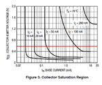
For me something in your explanation does not fit to the folowing chart (which is from the Fairchild BC546 datasheet).
bjt.PNG
I draw the red line. It is the expected V_BE when the BJT is in its usual operating point.

Now let´s focus on the area below the red line.
It is the area where the potential of the base is lower than the potential of the collector.

This chart clearely shows: the collector current is way higher than the base current although VBE < VCE.
IC = 10mA --> IB dwon to 0.025mA (b = 400)
IC = 20mA --> IB down to 0.05mA (b = 400)
IC = 50mA --> IB down to 0.25mA (b = 200)

*****
Certainly, there is a base current and in most cases we consider it (Ib=Ic/beta) during resistor calculations. But it has no control function at all.
It simply does exist - as a kind of by-product - because only 95...99% of the charged carriers reach the collector (and the rest goes to the base forming the base current).

Maybe a misunderstanding: Do you really say the collector current controls the base current?

Then how can a emitter follower circuit act as an amplifier?

***
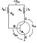
Here a picture from wikipedia: https://en.wikipedia.org/wiki/Bipolar_transistor_biasing
Fixbias.png
two scenarios:(start with bjt biased in a way that VCE = VCC/2)
1) change Rb to change IB --> I´d say this has the effect that IC changes, too. (according b at this operating point)

2) change Rc to change IC --> I´d say this has about no effect on IB. (far away from b)

***
Finally I have to admit that I have a only small clue about bjt inside physics.
(But my mathematics matches to my (maybe false) knowledge).

Klaus
 

Hi,
I´m really surprised by your explanation.
I wonder why you take your focus on collector current ... and the same time it seems you ignor that all the collector current goes through emmitter, too.
So I´d say: If the base (current) influences collector current, then it also influences emitter current. --> the collector current can not flow in a single point.
Klaus

Klaus - at first, I did not ignore the emitter current (see the first line of my former answer).
Secondly, the last sentence of the quoted part above ("If the base current....") is just a claim without evidence - and it is wrong.

For me something in your explanation does not fit to the folowing chart (which is from the Fairchild BC546 datasheet).
View attachment 133491
I draw the red line. It is the expected V_BE when the BJT is in its usual operating point.
Now let´s focus on the area below the red line.
It is the area where the potential of the base is lower than the potential of the collector.

Below the red line the voltage VCE is smaller than 0.6V. How can you say that the "potential of the base is lower than the potential of the collector" ?
Just the opposite is true.

Maybe a misunderstanding: Do you really say the collector current controls the base current?

Where did I say this? Do you even think that an expression like Ib=Ic/beta implies any statement regarding cause and effect?

two scenarios:(start with bjt biased in a way that VCE = VCC/2)
1) change Rb to change IB --> I´d say this has the effect that IC changes, too. (according b at this operating point)
This view is too simplified. What really happens is the following:
The current IB goes through the resistor RB and the B-E path of the transistor.
Hence , we have a voltage division between two resistances: RB and RBE=VBE/IB (static DC resistance).
Now - changing RB will change the division ratio and, thus, the voltage VBE.
And THIS is the effect that matters! Don`t forget: A current and changes of currents are always the RESULT of voltage changes!

In short: RB changes have an influence on the voltage division ratio and, therefore, on the voltage VBE (which - in turn - changes the emitter resp. collector current).
Of course, there is also a change of IB, but this is the RESULT of the voltage variations and not its cause.
The base current IB does exist (as a "by-product") but has no control function.
2) change Rc to change IC --> I´d say this has about no effect on IB. (far away from b)
Why do you think that a change in Rc would change Ic? This is not the case! (neglecting minor effects).
 
  • Like
Reactions: CataM

    CataM

    Points: 2
    Helpful Answer Positive Rating
Hi,

I must say I'm confused, because your explatation sometimes says the opposite of what I've learned.
I really can't follow your explanations. About potential...why 0.4V is more potential than 0.6V for example...maybe you don't talk about voltage potential...
Why you talk abot Rbe as an ohmic resistor in a voltage divider configuration. In my eyes Vbe is rather constant than it varies with base current.
And a lot of other confusions.

Wikipedia says:
Voltage, current, and charge control
The collector–emitter current can be viewed as being controlled by the base–emitter current (current control), or by the base–emitter voltage (voltage control). These views are related by the current–voltage relation of the base–emitter junction, which is just the usual exponential current–voltage curve of a p-n junction (diode).[2]

Maybe there is more than one explanation.

Maybe your explanation is more correct in terms of the true physical behaviour. I really don't know.
But in this forum it assume it more confuses than it helps - especially the newbies and hobbyists (and at least me)

Best is if the OP decides if your explanations are usefull or if the usually taught -simplified- calculation model is usefull.

Klaus
 

Hi,
I must say I'm confused, because your explatation sometimes says the opposite of what I've learned.

I know. I am aware that some books (and profs) claim that Ib would control Ic. But this is simply wrong. If you like I can give you some serious references (including W. Shockley - the famous "inventor" of the equation which describes the voltage-current relation across the pn junction).

Hi,
I really can't follow your explanations. About potential...why 0.4V is more potential than 0.6V for example...maybe you don't talk about voltage potential...

Did you realize that VCE (and NOT VBE) is shown in the figure you have copied in post#11 ?

Hi,
Why you talk abot Rbe as an ohmic resistor in a voltage divider configuration. In my eyes Vbe is rather constant than it varies with base current.

...rather constant? Did you ever hear about the exponential relationship between VBE and IC? The slope of this curve is the transconductance gm - the main parameter which determines the voltage gain of an amplifier!

Wikipedia says:
.........
........
Maybe there is more than one explanation.

You should not blindly rely on Wikipedia. More than that, they say: "....can be viewed as being controlled..." (a rather weak wording).
No - there is only one single correct explanation. Can you explain the working principle of the following cirucits based on current-control ?
Current mirror, differential amplifier, log. amplifier, VBE multiplier, class-B or class-C power stages,...

Maybe your explanation is more correct in terms of the true physical behaviour. I really don't know.
But in this forum it assume it more confuses than it helps - especially the newbies and hobbyists (and at least me)

For my opinion, a correct answer can confuse somebody only when (a) he has learned a simplified (but wrong) principle and (b) if he is not willing to improve his knowledge.
Having this in mind, such a confusion could be a good starting point for reconsidering some things, don`t you agree?
More than that, in his post#6 the questioner explicitely has asked for a "physical explanation". Do you recommend to give him wrong explanations?

Some final questions:
Do you really never review or verify - from time to time - your present understanding ?
Don`t you see any relation between the working principles of a pn diode and the transistor?
Do you have really no problems to believe that (simple example) one charged carrier which enters the base region should be able to release and influence more than 100 charged carriers forming the collector current (assuming a beta-value of >100)?
 
Last edited:

Hi,

Don't start a personal fight.
It's the OP's thread.

Klaus
 

Hi,
Don't start a personal fight.
It's the OP's thread.
Klaus

Klaus - please stay fair.
It was YOU who has claimed that I would confuse somebody (instead of giving some help).
More than that, it was the OP who has asked for additional explanations, right?
Did you overlook these facts?
 

Hi,

I always admitted that there may be several explanations.
I'm not the friend of "black or white".
Therefore I leave it on the readers which explanation to choose.

I stop discussion here.

Klaus
 

The most erroneous stories are those we think we know best--and therefore never scrutinize or question.
-Stephen Jay Gould
 

Status
Not open for further replies.

Similar threads

Part and Inventory Search

Welcome to EDABoard.com

Sponsor

Back
Top