Continue to Site

Welcome to EDAboard.com

Welcome to our site! EDAboard.com is an international Electronics Discussion Forum focused on EDA software, circuits, schematics, books, theory, papers, asic, pld, 8051, DSP, Network, RF, Analog Design, PCB, Service Manuals... and a whole lot more! To participate you need to register. Registration is free. Click here to register now.

Input Impedance of Multiplier diode

Status
Not open for further replies.

kamranraja222

Member level 1
Joined
Sep 25, 2011
Messages
37
Helped
0
Reputation
0
Reaction score
0
Trophy points
1,286
Activity points
1,589
Hello everyone,

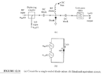
My question is "how to find an input impedance of a Multiplier PIN diode?." I am using HSMP-3822 diode to make an X3 multiplier. My input signal is 100 MHz and output is 300 MHz. The input signal power is 10dBm and a bandpass filter is also used at the output port. Thanks and best regards
 

Now I am using VNA to measure the input impedance of multiplier diode(PIN diode). It shows different input impedance for two cases:
1: when I connected VNA at input port of diode and connect the BPF at the other port of diode.
2: when I connected VNA at input port of diode and terminate the other port with 50 ohm termination.

Which one is correct configuration? Thanks
 

Now I am using VNA to measure the input impedance of multiplier diode(PIN diode).
Do you have frequency offset option in your VNA ?
If not, it is meaningless to connect output of mixer to port-2.

It shows different input impedance for two cases:
1: when I connected VNA at input port of diode and connect the BPF at the other port of diode.
2: when I connected VNA at input port of diode and terminate the other port with 50 ohm termination.
Which one is correct configuration?
1 is correct, if output of BPF is terminated correctly.
 
Last edited:
I think my VNA has no frequency offset option. I only connected one port of VNA to the input of diode. The output of diode is connected with BPF(which is terminated with 50 ohm termination).Moreover diode is connected towards ground.
 

How do you feed local signal to diode ?

VNA has a power range from 0dbm to 10dbm. I set the power level of 9dbm. This multplier diode dont need seperate dc biasing. The purpose of all this exercise is to match the input port of multiplier diode. Am I doing right so far??
 

Is your mixer a signle diode type like attached figure ?
 

Attachments

  • 160612-000231.png
    160612-000231.png
    22.2 KB · Views: 133

Yes like this but without any dc bias. One thing I should mention that this diode act as a multiplier no as a mixer.
 

Sorry.
Your configuration is a tripler not multiplier.
So input is a just one.

Vin**2 is a doubler.
Vin**3 is a tripler.
They are all not called as multiplier.

VNA has a power range from 0dbm to 10dbm.
I set the power level of 9dbm.
This multplier diode dont need seperate dc biasing.
The purpose of all this exercise is to match the input port of multiplier diode.
Am I doing right so far??
Right.
 
Last edited:
I am not getting your last comment.Please explain it more. Yes the mentioned equations are correct
 

Generally multiplier means two inputs and one output system like v3=v1*v2.

You should use a term of "Frequency Multiplier".
Both "Doubler" and "Tripler" are "Frequency Multiplier".
 
The HSMP-3822 is a PIN diode. The "I" in PIN means there is an energy storage "intrinsic layer" that will make this diode work a little like a "Step Recovery Diode". In other words...it multiplies because it is a highly nonlinear device. That is Idiode= (a very nonlinear function of the input voltage).

So simply hooking the diode to a VNA is NOT going to simulate the correct LARGE SIGNAL conditions of the diode when it is properly running. i.e. when there is an input matching/lowpass filtering mechanism, when there is some sort of 2nd harmonic tuning (idler frequency tuning), and when there is a highpass/matching network on the output. So a VNA will tell you not too much, even IF you could get enough power out of the VNA.

SO, you have two methods to get at the impedance of the diode when it is operating properly terminated:
1.) Calculate the effective impedance from some past papers. There is a book by Penfield and Rafuse that explains the equivalent impedances at Fin, 2Fin, and Fout.
http://techdigest.jhuapl.edu/views/pdfs/V04_N2_1964/V4_N2_1964_Thompson.pdf
There is also a classic HP application note 920 on step recovery diode multipliers.
I can give you half of the answer, the effective capacitance is approximately Ceffective = 2 X (the capacitance at Vbreakdown). For the real part of the input impedance of the diode, refer to the above papers
or
2) use a non-linear analysis program to calculate it all for you with a non linear simulation. However, usually these programs have a very poor model for a step recovery diode (do not include the charge storage mechanism) and therefore can give questionable results.

- - - Updated - - -

this program might yield a good start point for a nonlinear analysis:
http://www.flambda.com/srd.html
 
Last edited:
The HSMP-3822 is a PIN diode. The "I" in PIN means there is an energy storage "intrinsic layer" that will make this diode work a little like a "Step Recovery Diode". In other words...it multiplies because it is a highly nonlinear device. That is Idiode= (a very nonlinear function of the input voltage).

So simply hooking the diode to a VNA is NOT going to simulate the correct LARGE SIGNAL conditions of the diode when it is properly running. i.e. when there is an input matching/lowpass filtering mechanism, when there is some sort of 2nd harmonic tuning (idler frequency tuning), and when there is a highpass/matching network on the output. So a VNA will tell you not too much, even IF you could get enough power out of the VNA.

SO, you have two methods to get at the impedance of the diode when it is operating properly terminated:
1.) Calculate the effective impedance from some past papers. There is a book by Penfield and Rafuse that explains the equivalent impedances at Fin, 2Fin, and Fout.
http://techdigest.jhuapl.edu/views/pdfs/V04_N2_1964/V4_N2_1964_Thompson.pdf
There is also a classic HP application note 920 on step recovery diode multipliers.
I can give you half of the answer, the effective capacitance is approximately Ceffective = 2 X (the capacitance at Vbreakdown). For the real part of the input impedance of the diode, refer to the above papers
or
2) use a non-linear analysis program to calculate it all for you with a non linear simulation. However, usually these programs have a very poor model for a step recovery diode (do not include the charge storage mechanism) and therefore can give questionable results.

- - - Updated - - -

this program might yield a good start point for a nonlinear analysis:
http://www.flambda.com/srd.html

If I may, I would add some practical notes.

The PIN or SRD diode multipiers operate as parametric devices. I saw some attempts to calculate input impedance but it never worked. The truth is that you need a wide-range input impedance matching device, like a series-parallel variable capacitors, to achieve a good efficiency.
The DC bias is essential to make the parametric multiplier work, and a variable resistor adjustable to 1 k - 100 kOhm is needed.
Typical input power must be + 17 dBm or higher, otherwise no good output is generated.
The parametric SRD multiplier requires three resonant circuits coupled to the diode : input, output and IDLER. If properly adjusted, tripler efficiency better than 10 dB can be achieved.
Parametric frequency multipliers are only good for one-frequency input and cannot be tuned over a wider range, typically less than 1 per cent the center frequency.
Not all diodes operate well, it is often needed to select from say three-five units of the same type.

If you need an easier design, use mixer diodes as fast alternating switches. Mount a pair front-to-back, feed it +17 dBm. Only input and output resonants circuits are needed, a well-tuned tripler has some 10-13 dB loss.

I made many parametric multipliers at 10 to 100 GHz range, and I know what it is about. The growing demand for wideband multiplers caused our and other companies to stop making these nice devices. They are now replaced by "active" multipliers that use passive diodes plus power amplifiers. They are nice but with the wideband amplifiers they generate noise which is bad in receivers.
 
Even if the PIN or SRD diode multipiers operate as parametric devices, we can measure large signal s11 by VNA as far as configuration as frequency multiplier is complete.

Here "complete" means all circuits necessary for proper mode operation are euipped at both input and output.
 
Even if the PIN or SRD diode multipiers operate as parametric devices, we can measure large signal s11 by VNA as far as configuration as frequency multiplier is complete.

Here "complete" means all circuits necessary for proper mode operation are euipped at both input and output.

If you use a standard VNA, it generates a low power for which a SRD multiplier would need an external DC bias to operate. Parametric SRD multipliers usually run at +17 dBm or more, and rectify their DC bias on an adjusted resistor for the optimum perfomance.
 

Parametric SRD multipliers usually run at +17 dBm or more
See start of this thread.
This tripler can work for input=10dBm@100MHz and output=300MHz.

I don't think this tripler work as parametric circuit.
Simply it works based on I-V nonlinearity.
 
Last edited:

See start of this thread.
This tripler can work for input=10dBm@100MHz and output=300MHz.

I don't think this tripler work as parametric circuit.
Simply it works based on I-V nonlinearity.

I would disagree. The I-V nonlinearity of a SRD generates a wide frequency spectrum like a spark gap, and if you filter only the third harmonic, the efficiency will be quite poor. This is why Manley-Rowe equations apply for non-linear variable capacitance elements.
This is why I would recommend to use a pair of mixer diodes as a reasonable multiplier.
 
Status
Not open for further replies.

Part and Inventory Search

Welcome to EDABoard.com

Sponsor

Back
Top