Continue to Site

Welcome to EDAboard.com

Welcome to our site! EDAboard.com is an international Electronics Discussion Forum focused on EDA software, circuits, schematics, books, theory, papers, asic, pld, 8051, DSP, Network, RF, Analog Design, PCB, Service Manuals... and a whole lot more! To participate you need to register. Registration is free. Click here to register now.

[SOLVED] OTA Folded Cascade design procedure

Status
Not open for further replies.
For sure it makes sense to simulate the step response of your design to look at the slew rate and also to check the stability of the system in time-domain. Get your circuitry to the worst condition -> follower. No ringing should occur at the output node.
 
Ok. So I should put in and out together again and put a step leaving common mode voltage right?
 

Right.. with this condition the design has to handle the worst condition. Just apply a step from VSS to VDD at the input. You can also have a look at different corners (ss,ff..). Let's see what happens ;)
 

I tried to set up simulation like this but it seems like it isn't working. Have I done something wrong there? OTASTEP.PNG
 

you apply 1 volt amplitude to your input, thats too much !

- - - Updated - - -

change it to 1 mv

- - - Updated - - -

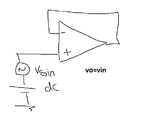
moreover, why did you connect your output to dc voltage ??? I do not get it !
 
Hi Ata_sa16,
Thank you for your answer. I have made that connection just as if I was using an OPAMP in voltage follower configuration but as I think I pointed out before, I'm not sure of it. It's the first time doing an analog project so I make lots of mistakes, thanks you for your patience, gonna try it again this evening!
 

Ok, here I am. I connected as you told me to, here is the circuit /w the simulation results. Assuming this one is correct, what would I have to do to correctly calculate slew rate? I mean, should i consider the point when the output reaches the stable value or just evaluate the slope of the ramp from the point where it starts to the point when it reaches the input value for the first time? Moreover, I thought I could give an ideal step as an input, but I dont seem to be able to.

OTASTEP2.PNG

OTASIMUSTEP.PNG
 

Ok Do you want to measure slew rate ?

- - - Updated - - -

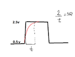
yes for single ended you have to measure 10% to 90%

- - - Updated - - -

it is V/uS you measure voltage difference then you measure time and calculate V/t

- - - Updated - - -

And also your biasing system is kind of wrong for folded cascode OTA. Its not reliable. For simulation it is ok but in real life you need to design more advanced bc its affected from variations like temperature.

- - - Updated - - -

also increase your input transistor sizes for better Gm and gain and decreasing the noise.

- - - Updated - - -

make those 17.5u something around 30-40u

- - - Updated - - -

you are working with 3.3 volt

for slew-rate apply voltage from 0.5 to something around 2.5 pulse and then measure.

- - - Updated - - -

apply this in input

Untitled.png
 

Thank you for your answers, they really come into help. When you say "And also your biasing system is kind of wrong for folded cascode OTA. Its not reliable. For simulation it is ok but in real life you need to design more advanced bc its affected from variations like temperature.", what is the cause for it?
 

well the design should be in a way that your bias system and transistors should be affected from temperature and vdd variation in a same way, its kind of complicated. you can find in reference books.
 
Ok thank you, just wanted to know if there was some evident reason, I'll check
 

For OTAs it is common to analyse over three corners:

1) The design is done within the typical-typical corner with the nominal temperature -> 27°C.
But you have to include margin to get even within the worst case in spec.

2) Best case: corner fast-fast (NMOS - fast, PMOS - fast) with the highest temperature of your spec -> ex.: 120°C.
Your circuitry is as fast as possible -> higher BW, gain due to larger currents

3) Worst case: corner slow-slow (NMOS - slow, PMOS - slow) with the lowest temperature of your spec -> ex.: -50°C
Your circuitry is as slow as possible -> you have to be still in spec


https://en.m.wikipedia.org/wiki/Process_corners

BR

Edit: To estimate your yield apply Monte Carlo Analysis including mismatch to your design
 
Last edited:
Hi, I have made the simulation for the input step as you told me to, this is the result: the hand calculated SR is very near to that value (considering 10%-90%)

OTASTEP6APR.PNG
 

Thank you for your answer erikl, but my SR is now 30 V/us since I have remade the project from the first time I posted it.

-Edit: I saw now that you said 30 uV, but the Y axis is in Volts, so shouldn't it be V/us?
 
Last edited:

... the Y axis is in Volts, so shouldn't it be V/us?

No: the usual presentation of transient analysis results is in [value] vs. [time], so your diagram [voltage] vs. [time] is correct.

It wouldn't make much sense to display [slew rate] vs. [time], would it?
 
Yes, of course, what I wanted to say is that in your message you told that it appears to be of 30[uV/us] while for me it's about 28 [V/us] and since I tend to recognize that I probably have 0.1% of your experience in analog design, I still can't get how it could be so low: I just made (90% [V] - 10% [V]) / (60ns = 0.06 us) = 1.6 [V] / 0.056 [us] = 28.6 [V/us]
 

Status
Not open for further replies.

Similar threads

Part and Inventory Search

Welcome to EDABoard.com

Sponsor

Back
Top