Continue to Site

Welcome to EDAboard.com

Welcome to our site! EDAboard.com is an international Electronics Discussion Forum focused on EDA software, circuits, schematics, books, theory, papers, asic, pld, 8051, DSP, Network, RF, Analog Design, PCB, Service Manuals... and a whole lot more! To participate you need to register. Registration is free. Click here to register now.

Hard switched bridge spiking even after snubber

Status
Not open for further replies.

mrinalmani

Advanced Member level 1
Joined
Oct 7, 2011
Messages
463
Helped
60
Reputation
121
Reaction score
58
Trophy points
1,318
Location
Delhi, India
Activity points
5,285
Hi
I have a hard switched MOSFET bridge running at 100KHz.
The output capacitance is nearly 5nF and the ringing frequency at transients is 48MHz.
After snubbing the FETs with an RC snubber of 20nF and 1 Ohm, ringing is damped out but a small spike of around 2V remains.
However when I begin to load the bridge, the spike rises to over 15V at 25A current.
No value of resistance or capacitance seems to suppress this spike.
IMG_20160303_215650.jpgIMG_20160303_215714.jpg
The two photos show the output at 10A load and 25A load.

The bridge drives a 12V : 240V transformer with approx 100nH leakage. The HV side of the transformer is connected directly to a resistive load without rectification.

How to solve this? Please help
 

The snubber dissipates energy as heat. The more power the load takes, the more the snubber the is stressed. Because some of the energy is coming back to the input side, instead of going into the secondary.

You can soften the blow by increasing the gate resistance a little. The mosfet will not turn on so hard and it will dissipate slightly more energy as heat and the snubber will be saved from that.

There are ways in which the snubber energy is used in a constructive way but I do not know. I have only heard about that. It is used like a flywheel.

Brute force always works but only upto a limit...
 
  • Like
Reactions: pes68

    pes68

    Points: 2
    Helpful Answer Positive Rating
Setup isn't clearly specified. What is it? H-bridge? You're apparently measuring voltage across transformer winding. How? Differential probe?

Presumed the ringing at the bridge output is real, the measurement shows that either the DC bypass capacitors or the bridge itself have too much parasitic inductance. So we need to look at the bridge geometry.

Seeing no effects of RC snubbers suggests that you didn't dimension them correctly. R should have the same order of magnitude as the characteristic impedance √(L/C) of the parasitic resonator, RC time constant moderately larger than the ringing period.
 

The spiking is at turn off, so it is the leakage L of the Tx plus any wiring inductance causing the spike, so you could solve by: a better Tx, less loop area in the wiring of the H bridge, a decent amount of high quality capacitor across the 12V to soak up the return of energy from the leakage L (the 25 amps has to go some where when you turn the fets off - through the anti-parallel diodes of the other fets and into the rail caps...!)
 

Sorry for late response.
This is a full bridge circuit connected to a new 12V 150Ah lead acid battery.

It's not that the snubber doesn't work. The R value has been carefully calculated and it does a wonderful job in damping the oscillations at no load to partial load of about 15A. Different values of R has also been checked for.
The problem comes as current increases. May be the wire connecting the transformer to the H-bridge output is too long? But the leakage inductance should easily bleach the effect of the cable inductance. A higher turn ratio transformer causes larger ringing, maybe Winding capacitance?
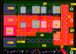
I am attaching photos of the PCB (a few components are missing).
There are nearly 20 ceramic capacitors (10uF) to stabilize the rail.
The bridge and the snubber are circled in red.
 

Attachments

  • Capture.PNG
    Capture.PNG
    833.8 KB · Views: 126
  • IMG_20160316_174127.jpg
    IMG_20160316_174127.jpg
    190.8 KB · Views: 108

May be the wire connecting the transformer to the H-bridge output is too long? But the leakage inductance should easily bleach the effect of the cable inductance.
Where do you probe the bridge output voltage? The cable only matters if you are probing at the transformer side which would be pretty useless. By the way, the photo gives the impression that you are intentionally increasing the wiring inductance by keeping both wires at a large distance instead of twisting it closely.

Presumed the bridge output voltage is probed directly at the bridge, suitable probe ground connection can be an issue, too. You may measure spikes that don't exist at the actual bridge output nodes.

It's difficult to guess from the PCB top view if the ground and input voltage planes and output nodes are arranged properly to minimize the wiring inductance. We would need to see the gerber data of all layers.
 

Here is a simulation of your Full bridge, 12vin, 240vout, 150W = Pout, Fsw=100khz.
You can play with putting in strays and snubbers etc and see if you can imitate what you see on the scope.
As discussed, you need to make the high di/dt feedback loops as narrow in area as possible.
Also is pdf of schem, and excel design file.
(sim is in ltspice and just needs converting to .asc then run it)

for noisy signals , you really need a 1:1 bit of coaxial cable to probe them with, not a scope probe with a dangling lead.

- - - Updated - - -

Also, here is attached PCB layout document for SMPS
 

Attachments

  • Full bridge _12vin 240vout 150w.pdf
    23.8 KB · Views: 120
  • FULL BRIDGE _12VIN 240VOUT 150W.zip
    2.7 KB · Views: 87
  • Full bridge _12vin 240vout 150w.TXT
    13.5 KB · Views: 56
  • Basics of SMPS Layout _4.doc
    645.5 KB · Views: 110
The high ringing frequency of 48MHz suggests a parasitic source and you need to reduce (dI/dt) a little bit- just sufficient to reduce the ringing at the max current load. The simplest way is to increase the gate drive resistance slightly- the power transistors will get bit hotter but hopefully not much. This too can be tried out in your simulation experiment.
 
In your top post it looks to me like you don’t have any dead time in the switching of your full bridge transistors. This as you know is not advisable.
Also, 1 ohm and 20nF sounds too dissipative for your RC snubber. As you know, in SMPS, its not necessary to totally snub out every bit of ringing that exists.
 
Yes, check the dead time between one fet turning off and its mate turning on - should be at least 100nS of dead time there, experiment with higher dead times.

If this is OK try turning the fets off a bit slower...

- - - Updated - - -

Also twist the wires together running to the Tx, i.e. minimise the loop area you are driving (lowest wiring inductance)

- - - Updated - - -

Also I would try 10nF and 3.3 ohms across each fet, for higher currents/powers you will need more aggressive snubbing - that's how it works, assuming the dead time is OK.
 

Yes, there is no dead time. But the driver ADP3120A applies an adaptive dead time to prevent shoot through, perhaps that wasn't sufficient.
I inserted a 100ns dead time in the PWM signal itself and the spike totally dissappered at no load. I could only test half the bridge. I have run out of gate drivers, they will be arriving in a day or two.

Does this imply that there must have been a shoot through prior to inserting the dead band? Or is there some other reason why a dead band would damp spikes?

- - - Updated - - -

The transformer wires are made long intentionally.

CopperTop.PNG

TopBottom.PNG

CopperBottom.PNG
 

no dead time gives you a sharp build up of current in the devices before one has to turn off, hence a bigger turn off spike as a result of too little dead time...
 
Thanks for showing the layout. The 2-layer design can't achieve perfect bus voltage bypassing, particularly C45 to C52 connected to the lower leg of the B+ "U" have much series L. I don't see an easy way to make it much better on two layer, perhaps except for a double side populated design with low and high side switches back-to-back.

Regarding sufficient dead time, you would either adjust the dead time and check if switching behavior and/or losses improve, or measure transistor currents directly (e.g. using rogowski coil or miniature CT).
 
Also your thermal vias look very close, maybe too close for your pcb fabricator?
But also, the full bridge has very high duty cycle, I am wondering if the sim and schem I offered in post#9 is actually what you are doing? ie, is it actually a Full Bridge SMPS or something else.
 

Also your thermal vias look very close, maybe too close for your pcb fabricator?
He was able to make it, so apparently - no.

The transformer wires are made long intentionally.
Length isn't a problem, the question was if you intentionally increased the inductance by not twisting the wires. The loop inductance adds to transformer leakage, it's probably a multiple of 100 nH. But it only causes spikes on the transformer side, not the H-bridge.

If you measure output voltage at the bridge side, you don't see it.
 

Thanks for the replies.
(Voltages are measured at the bridge side not the transformer side)

This is actually going to be a four layer board, we made two layers just for testing. Before jumping to a 4 layer PCB, I want to try out other possibilities in a 2 layer board.

The voltage across any individual capacitor (measured directly across the capacitor terminal) is relatively stable, but as we probe even half an inch away from the capacitor terminals, the problem starts.
The total stray inductance calculated from ringing frequency is 7nH. Even in a 4 layer PCB, I guess it will be difficult to reduce the stray significantly below 7nH.

Quick calculations show that these spikes do NOT have a lot of energy. However they are easily banging down the power MOSFETs. I have replaced over 50 failed MOSFETs with pulse rating as high as Idm = 1300A. Perhaps clamping each MOSFET with a suitable TVS may help?

Will ZVS help? How about phase shifted PWM?

@Treez
Thank you for all the files.
I installed that simulation software, however I dont know how to run simulation files on it.
 

to run the simulation, you need to turn the .txt file into a .asc file, then it can be opened in the free ltspice simulator.
Just open it and click the running man icon, and it will start running.

Are you sure its not just scope noise and the fets are blowing from overheating, or too much ringing on the gate drive etc?
There is a lot of current flowing in your fets.
 
No, definitely not.
FETs are not blowing off due to over heating. Although there's a lot of current, Rds(on) is less than one mOhm. FETs run cool enough to be touched.
 

Status
Not open for further replies.

Part and Inventory Search

Welcome to EDABoard.com

Sponsor

Back
Top