Continue to Site

Welcome to EDAboard.com

Welcome to our site! EDAboard.com is an international Electronics Discussion Forum focused on EDA software, circuits, schematics, books, theory, papers, asic, pld, 8051, DSP, Network, RF, Analog Design, PCB, Service Manuals... and a whole lot more! To participate you need to register. Registration is free. Click here to register now.

understanding the schematics

Status
Not open for further replies.

--BawA--

Advanced Member level 1
Joined
Nov 28, 2012
Messages
479
Helped
43
Reputation
86
Reaction score
42
Trophy points
1,318
Location
Noida, INDIA
Activity points
4,926
charger.png
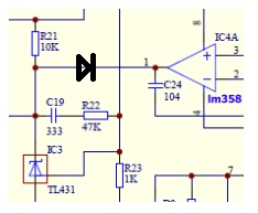
can anyone explain the working of the OUTPUT SECTION of the attached schematics in detail,
1) i mean , how current adjustments are done and what is the range of current adjustments?
2) working of tl431(ic3) , range of output voltage?
3) output of IC4A and input voltage range of pc817 opto?
4)working of IC4B.
 

IC4B just lights up some LEDs: D9 = normal operation; D10 = overcurrent condition (D11 it's an output voltage indicator).

R19 (0.02ohm) is the current sense resistor. When the output current reaches 10A, the voltage drop across R19 is 0.2V so IC4A switches its output to low (IN+ of IC4A is adjusted to 0.2V in that schematic - using R30 pot).

The forward current of IC2 optocoupler is increasing thus the Vref pin of U2 (UC3842) is modified, reducing the PWM duty cycle.

IC3 (TL421) it's an adjusted voltage reference which keeps the optocoupler biased in standby mode, to control the output voltage (using R24 pot).

- - - Updated - - -

D13 are used for battery reverse polarity protection and Q2/Q4 are used for battery presence detection and shortcircuit protection.

As long as the output is not connected to a battery, Q2 is in cut off state thus Q4 is also turned off and there's no current path through GND.

When you connect a battery (with a minimum voltage of 9-10V) the Q2 goes into saturation mode thus Q4 is turned on, allowing an output current path to the ground (normal operation).

If there's any shortcut condition on the output (between OUT+ and OUT-) the Q2 is turned in cut off state, turning off the Q4 MOSFET thus isolating the output current path to the ground.
 
Last edited:

Also I guess there is an error in the schematic. A diode is required in the connection between the output of IC4A and the cathode of IC3. See the picture below.

 
Yes, LM358 doesn't have an open collector output stage so that diode is mandatory (most probably, the original schematic had open collector comparators).
 

red_alert
1) how the values of r21 , r16 ,r27 , r30 are calculated?
2) if the current flowing in the battery is less than 0.5A , the output of the charger should trigger to 13.65V , is it possible using an OPAMP?
 

R30 (pot) and R29 represents an adjustable voltage divider, to set up the max output current threshold. The voltage at IN+ of IC4A opamp should be equal with I_OUT x R19 (I_OUT is the maximum output current).

R16 limits the current through IC2 (optocoupler).

R21 represents a biasing path for IC3.

R27 (and R20) represents a voltage divider for the output voltage. When Vout is greater than 14.4V, the IN+ of IC4B rise over 2.5V (IN-) thus signaling that maximum voltage.

IN+ = 14.4V * 4.7K / (4.7K + 22K) = 2.53V

- - - Updated - - -

if the current flowing in the battery is less than 0.5A , the output of the charger should trigger to 13.65V , is it possible using an OPAMP?

Whilst it's quite fun to play with opamps, these days it's way easier to use a cheap MCU to replace tens of opamps in a circuit like this.

Anyway, I guess you don't want to go this route so that's my last warning. ;)

About your question: you have to check (compare) the voltage across current sense resistor (R19) using an opamp and the output voltage, using another opamp. When both condition are true (I_out < 0.5A and V_out > 13.65V) you have to trigger the IN- of IC4A, to further control the U2 (to decrease the PWM duty cycle).
 

Actually i want to learn the opamps completely thatswhy i am designing these circuita with opamps,
btw , if i use any microcontroller for an offline converter , can you help me to design a startup circuit for it , i mean , in uc3842, the startup voltage is somewhat around 18V , and can be vary in steady state so it's easy to design a startup circuit., But for a microcontroller , there should be clean 5V supply , so how to design a startup circuit for a microcontroller?
 

You could use any series voltage regulator (LM7805) for that.
 

Status
Not open for further replies.

Part and Inventory Search

Welcome to EDABoard.com

Sponsor

Back
Top