Continue to Site

Welcome to EDAboard.com

Welcome to our site! EDAboard.com is an international Electronics Discussion Forum focused on EDA software, circuits, schematics, books, theory, papers, asic, pld, 8051, DSP, Network, RF, Analog Design, PCB, Service Manuals... and a whole lot more! To participate you need to register. Registration is free. Click here to register now.

High frequency PCB layer stack guidance

Status
Not open for further replies.

viperpaki007

Full Member level 5
Joined
Jul 2, 2008
Messages
270
Helped
11
Reputation
22
Reaction score
8
Trophy points
1,298
Location
Finland
Activity points
3,395
Hi,

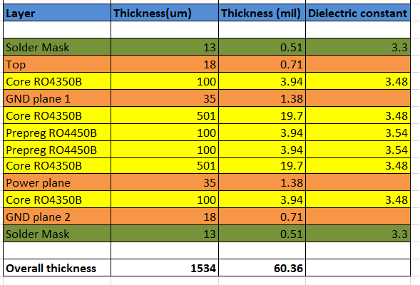
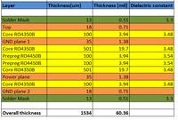
I am making an RF PCB (max frequency 8GHz). One manufacturer suggested the following layer stack for me (see attached figure). They use Rogers material as Rogers have good RF performance. My question: Is it necessary to use Roger material between central layers?. Central layers are used for Gnd and power plane and there are no RF signals routed on these layers so i am thinking that may be Roger material is not required between Central layers and only a FR4 material can work as well. Any comments?


Dear,
Your RF board have high power amplifier or microstrip filter circuits? If no,just use RF-4.
 

I have a differential 8GHz signal routed on RF top layer. I need controlled 100 impedance lines on the top layer.


Dear,
Your RF board have high power amplifier or microstrip filter circuits? If no,just use RF-4.
 

As you said, you do not need Rogers material between low frequency layers. You need the low loss material between top RF and its ground only, the other layers can have FR4.
 
Dear viperpaki007,
you can made differential 8GHz signal etch line as short as possible, via is less than 2/etch line, impedance controlled.Simulation optimization via may be perfect. all for RF-4 purpose.
 

You can use 3/8 oz. Cu on RO Dk for outer layers, 0.5 oz for Epoxy clad layers and 1 oz layers for Vcc and ground for strength on uneven etched signal layers to prevent warp.

Also 1oz gives lower conduction losses, and lower crosstalk with appropriate prepreg in between also. As well better tolerance on 3/8 Oz fine line copper over RO Dk. (ROgers Dielectric constant) but blind or buried vias adds cost to process to fabricate and verify reliability.

There are many types of epoxy/glass ratio FR4 and different weave patterns and. fill factors, whichaffects Dk andloss tangents greatly, vs GHz .
 

Status
Not open for further replies.

Part and Inventory Search

Welcome to EDABoard.com

Sponsor

Back
Top