Continue to Site

Welcome to EDAboard.com

Welcome to our site! EDAboard.com is an international Electronics Discussion Forum focused on EDA software, circuits, schematics, books, theory, papers, asic, pld, 8051, DSP, Network, RF, Analog Design, PCB, Service Manuals... and a whole lot more! To participate you need to register. Registration is free. Click here to register now.

problem with design footprint in allegro

Status
Not open for further replies.

asa1365

Member level 3
Joined
Nov 4, 2013
Messages
61
Helped
1
Reputation
2
Reaction score
1
Trophy points
8
Location
mashad
Activity points
398
Hello

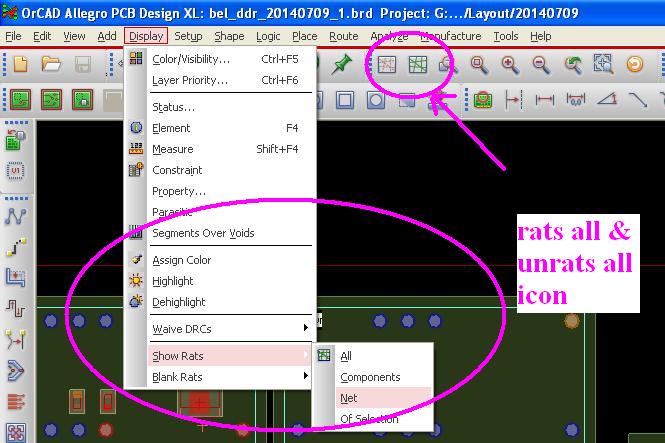
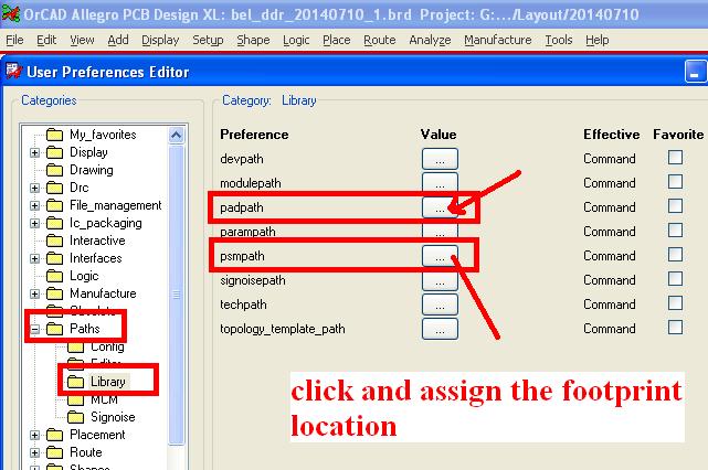
I design a footprint with allegro but when I import it to my board it have not connection with other parts and dose not get on my pcb .
can you guide me ?
Regards.
 

Hi
please check the pin number in schematic symbol and Footprint;both should be match with each other.while importing if you not get any error ;check rates net enable
 

pin number is A1,A2,....and like schematic .
how do i check rates net enable?
 

Hi,
check did u assign the same pin configuration for footprint.if not assign it.For rates net enable select rates all icon or display----> show rats-->all.you can find pins to be connected or not in near my components
 
I start Allegro 16.5 short-time . i designed a R603 symbol.now design a pci x1.
i can not find show rats in display , can you explain more ?

thank you
 

Hi asa,
First let me know what is PCi x1 ?? is it net ,symbol,or board name ?? RATS all (ICON may be is there). i am using allegro 16.2


i design footprint ,pci is a symbol pci.dra
i want to add it to my board .
i design footprint without wizard

rats are in files .brd
 

1.open your schematic,select the symbol then Right click ---->edit properties-->PCB Footprint --->paste your footprint (created footprint) and then generate netlist
2.open your board file and import it.
 

i do them but my footprint have a problem but i do not know
my footprint have not connection to other parts
it do not get on my board
can explain why is grid important ?
and explain what is important design a footprint ?
 

Hi
setup-->userpreference-->select the path-->library--pad path and psm path assign the footprint location new you can import the netlist

 
Hello....also make sure that the *.psm file is created with your *.dra file.
 
hi,
check the footprint name correctly.name should not match with other footprint.one again delete the netlist file and regenerate the netlist and then import it.it will work(your schematic symbol pins and footprint pin no should be match)
 
Status
Not open for further replies.

Part and Inventory Search

Welcome to EDABoard.com

Sponsor

Back
Top