Continue to Site

Welcome to EDAboard.com

Welcome to our site! EDAboard.com is an international Electronics Discussion Forum focused on EDA software, circuits, schematics, books, theory, papers, asic, pld, 8051, DSP, Network, RF, Analog Design, PCB, Service Manuals... and a whole lot more! To participate you need to register. Registration is free. Click here to register now.

What is the best phase margin for a loop?

Status
Not open for further replies.
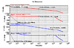
No its 87 .... PM is how much more phase shift is required to make the total phase shift of the system 180. For your case the system phase has already shifted by 93 so to make it unstable it will need 87deg more shift. So the margin left in your system is 87deg .... that is why we call it margin

I am afraid, your contribution is somewhat confusing.
Simulation results are: -180 deg. at DC and 87 deg. at unity gain. Hence, the difference to the stabiluty limit (0 deg or 360deg) is 87 deg. It is wrong to find the difference to 180 deg.

- - - Updated - - -

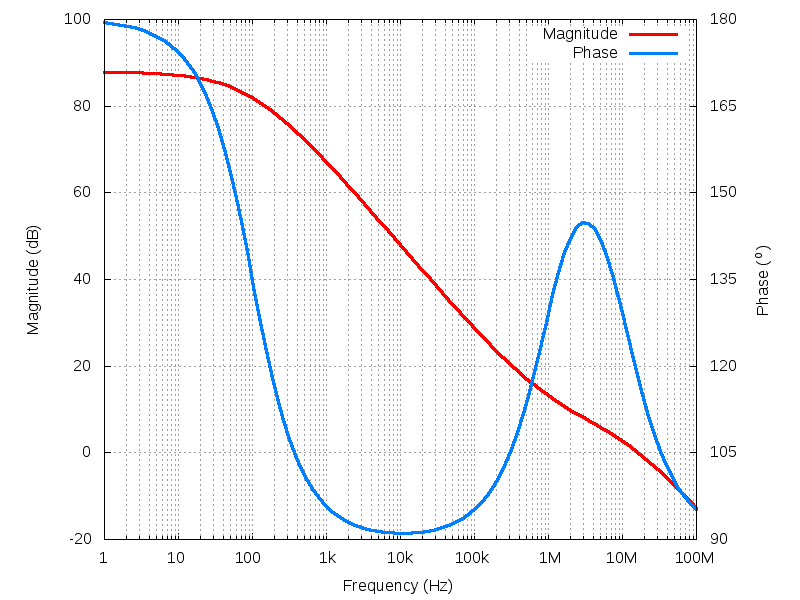
I just measured phase margin of LDO for a different case and now phase margin is 93 degree. But according to post #3, the maximum phase margin is 90 degree.
Is there something wrong here?

anhnha, are you sure? HOW did you measure?
In post#13 the margin was 87 deg - and now it is 180-87=93 deg?

- - - Updated - - -

the PM could be higher than 90 degrees, i.e. when transfer function contains low freq. dominant pole, LHP zero and nondominant pole after a next decade.

Yes - correct. In principle, it is possible that there is a phase enhancement due to a zero - however, I suppose this does not apply to the system under discussion.
Hence, I am not sure if anhnha does simulate the loop gain correctly.
 

anhnha, are you sure? HOW did you measure?
In post#13 the margin was 87 deg - and now it is 180-87=93 deg?
Hi.
I measured phase margin under different load conditions. I measured it by using a very large inductor and by injecting the signal with a large capacitor.
Phase margin now (93 degree) is the case with different load.
The phase starting from 180 degree and gain at 87 degree is 0dB. So, as you said above, phase margin will be 93 degree.
Yes - correct. In principle, it is possible that there is a phase enhancement due to a zero - however, I suppose this does not apply to the system under discussion.
Zeros will increase phase and so this is possible?
 

Hi.
I measured phase margin under different load conditions. I measured it by using a very large inductor and by injecting the signal with a large capacitor.
Phase margin now (93 degree) is the case with different load.
The phase starting from 180 degree and gain at 87 degree is 0dB. So, as you said above, phase margin will be 93 degree.

Where did I say that?
If you would introduce additional 87 deg into the loop you would be at 360deg (the stability limit). Thus, the margin you have is 87 deg.
I think this sounds logical, does it not?
Read again my post#14

(The contribution from SIDDHARTHA HAZRA is not correct).
 
  • Like
Reactions: anhnha

    anhnha

    Points: 2
    Helpful Answer Positive Rating
Well, sorry for my mistake.
I meant to say that at 93 degree gain is 0dB => phase margin = 93 degree.
I measured phase margin of LDO with different supply voltages and different load currents.
Most of them have phase margin from 65 to 87 degree but some has 93 or 91 degree.
I will try to use PZ (poles/zeros) analysis in Cadence to see if there is a zero like that.
 

The ideal situations is a single real LHP pole - for that situation the system is absolutely stable and step response is ~1-exp(-t·w0), where w0 is a pole frequency.
In general a transfer function could contains zeros and poles which are either left- or right-half plane and complex. The poles located in RHP causes instability always, while complex LHP poles a±ib gives damping oscillations which amplitude depend to Q factor of it (proportional to ratio between real and imaginary part of complex pole). The step response for system with complex LHP pole w=a±ib is ~1-exp(-t·a)(sin(b·t)+cos(b·t)) - for high Q factor (in general we have three solutions for damping oscillations).

The LHP zeros could be useful to eliminate non-dominant poles, while RHP zeros produces additional phase shift (like poles) but decreasing slope causing stability problems.

Well designed system shouldn't contains any zeros and has at most two poles, while non-dominant one should be around decade away from GBW frequency (every other poles and zeros should cancel each other).

//edit: heh, I didn't notice second page of thread ;-)
 
  • Like
Reactions: anhnha

    anhnha

    Points: 2
    Helpful Answer Positive Rating
I will try to use PZ (poles/zeros) analysis in Cadence to see if there is a zero like that.

If you don´t mind, it would be very helpful (in order to avoid misunderstandings or misinterpretations) if you would show the loop gain response (magnitude and phase, both vs. frequency).
From these figures it would also be possible to see if there are zeros.

- - - Updated - - -

And - yes - there could be a LHP zero, which could be caused by a finite ESR (loss resistance) of a capcitor across the load. Is this the case?
 
  • Like
Reactions: anhnha

    anhnha

    Points: 2
    Helpful Answer Positive Rating
Thank you.

Dominik Przyborowski and LVW.

Dominik Przyborowski:

Why it is not better to have a phase margin larger than 90 degree?
LvW:

And - yes - there could be a LHP zero, which could be caused by a finite ESR (loss resistance) of a capcitor across the load. Is this the case?
I put an ideal 1uF capacitor at output of LDO and an ideal current source to simulate load current. So there isn't any resistance from the capacitor.
Below is the gain and phase margin.
 

Attachments

  • Phasemargin_proLDO2.5V_Vin3.3_14Jun.png
    Phasemargin_proLDO2.5V_Vin3.3_14Jun.png
    11.9 KB · Views: 99

I am a bit surrised that the margin increases for full load.
On the other hand, the gain flattens out above app. 1 MHz - this is equivalent to a corresponding phase enhancement (caused by a zero). Hence, the margin can indeed be above 90 deg.

Question: Did you place the inductor at a node where a low output resistance sees a large load resistance?
Otherwise, your simulation is not correct because of loading errors.
Best place for simulation (placement of the inductor): Input or output of the opamp (error amplifier).
 
  • Like
Reactions: anhnha

    anhnha

    Points: 2
    Helpful Answer Positive Rating
Thanks. I don't have the circuit completely now but my circuit is really same the one below. However, my LDO has one buffer after folded cascode amplifier and one 1uF output capacitor.

I did gain simulation like that.
 

Attachments

  • LDO gain loop simulation.PNG
    LDO gain loop simulation.PNG
    149.2 KB · Views: 147

As far as I can see - the breaking of the loop seems to be OK (gate of M1).
 
  • Like
Reactions: anhnha

    anhnha

    Points: 2
    Helpful Answer Positive Rating
As far as I can see - the breaking of the loop seems to be OK (gate of M1).
Is the phase margin 93 degree good?
 

Dominik Przyborowski:

Why it is not better to have a phase margin larger than 90 degree?
Because the best response of the system we can obtain for single pole system. Below I attached small comparison of two systems with the same dc gain (88dB) and GBW (~16MHz) but one is single pole and other is two-pole and one zero (all real and LHP) with PM~120 degrees.
Bode plots of 2p-1z system (single pole is obvious so I didn't attach it) open loop and in buffer configuration:

buffer.png

And the most important - a step response:
step_resp.png
The above difference is caused by zero which swaping dominant pole in closed loop system.
In addition You get 93degrees of PM but in cost of gain margin.

LvW said:
I am a bit surrised that the margin increases for full load.
The PM increases due to higher transconductance of pass transistor which moves non-dominant pole.
 
Last edited:
  • Like
Reactions: anhnha

    anhnha

    Points: 2
    Helpful Answer Positive Rating
Is the phase margin 93 degree good?

It is "good" - if it is correct. But I don´t know because I am still not sure if you have determined the loop gain correctly.
I have seen the inductor and the coupling C - however, I still don´t know if you have used the correct nodes for loop gain determination.
Loop gain is the ratio of both node voltages left and right to the inductor. Did you show this ratio in yout diagram?
 
  • Like
Reactions: anhnha

    anhnha

    Points: 2
    Helpful Answer Positive Rating
Thanks, Dominik Przyborowski and LvW.

Loop gain is the ratio of both node voltages left and right to the inductor. Did you show this ratio in yout diagram?
Yes.
How to know what component causing zero?
 

How to know what component causing zero?
By calculate the transfer function. Assume single pole trnasfer function of error amplifier K(s)=k0/(1+s/p0), add small signal model of pass transistor, feedback and load elements. On the first look You have a zero bounded with C1 capacitor. Check on hand calculation that is sthing like 1/(2pi·C1·R1) or 1/(2pi·C1·(R1||R2))
The second zero is bounded with pass transistor, which dimensions causes non-negligible Cgd value and produce zero located at gm_mp/(2pi·cgd_mp).
 
  • Like
Reactions: anhnha

    anhnha

    Points: 2
    Helpful Answer Positive Rating
Thanks, Dominik Przyborowski and LvW.
Yes.
How to know what component causing zero?

anhnha, may I ask you what is the purpose of the capacitor across R1 ?
 

A realistic load case would add a load capacitance, I presume. It can be expected to reduce the phase margin dramatically and bring out the necessity of internal frequency compensation.

Secondly, I have difficulties to understand the phase/frequency plot in loaded case. Looks like there's gain plateau around 2 MHz without corresponding phase lead. Or is it hidden by the diagram text?
 

Thank you. I will try that.

anhnha, may I ask you what is the purpose of the capacitor across R1 ?
I took the ideal from this paper below.
**broken link removed**

(2.4 Power supply rejection, page 17)
or
http://dspace.mit.edu/handle/1721.1/45647

The paper says it is used to improve PSRR (power supply rejection ratio).
 

Status
Not open for further replies.

Part and Inventory Search

Welcome to EDABoard.com

Sponsor

Back
Top