Continue to Site

Welcome to EDAboard.com

Welcome to our site! EDAboard.com is an international Electronics Discussion Forum focused on EDA software, circuits, schematics, books, theory, papers, asic, pld, 8051, DSP, Network, RF, Analog Design, PCB, Service Manuals... and a whole lot more! To participate you need to register. Registration is free. Click here to register now.

Digital to analog converter PCB design

Status
Not open for further replies.

Ali Mohaidat

Newbie level 3
Joined
Apr 23, 2014
Messages
4
Helped
0
Reputation
0
Reaction score
0
Trophy points
1
Location
Arbela, Irbid, Jordan, Jordan
Activity points
26
hello guys.
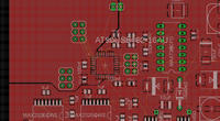
I am designing a PCB that contains a digital to analog converter , my question is about the separation between the analog and digital grounds i want you to take a look at my design and tell me what is best to do ,,
i have power supply that provides 3.3 volts , +-12 volts and 5 volts.
i used the 3.3 volts as a digital supply and the others all for the analog parts
i made a connection between the analog and the digital circuits under the dac , please look at the circuit and tell me the best way to separate between them in order to have the best performance .
thank you :)


U can use ferrite bead for separating analog signal from digital
 

Hi,

Confusing....I can't find a dac.

Klaus
 

Hi,

EAGLE: What DAC do you use? I also work with EAGLE and maybe i have a library with this part.
Without it you can´t use the schematic and the forward and back annotation between schematic and board layout.
I strongly recommend to use the schematic tool. It gives you a better view of your circuit and helps to avoid connection errors in board.

Regarding the GND: You have a good ground plane (much more better than single GND wires) so it looks good to me.
But to give you better assistance we need to know what sampling frequency, resolution and precision you like to achieve.

Good luck
Klaus


Thanx Klaus,,
I am using AD5764 ,, 16 bits 4 channels bipolar output voltage ,, i actually mapped the pins of the AT90 to the DAC am using ..
i am new in eagle i dont know much ,, please tell me what you think about the ground plane and whats best to do to have the best performance
this is the schem of the AT90 == my DAC
thanx alot again :)
<a title="2014-04-23_15-11-23.jpg" href="http://obrazki.elektroda.pl/4726627000_1398255326.jpg"><img src="http://obrazki.elektroda.pl/4726627000_1398255326_thumb.jpg" alt="2014-04-23_15-11-23.jpg" /></a>
 

The analog and digital ground planes can be common.But just make sure than you keep the analog and digital signals in separate areas and dont mix them up.
Google for mixed signal layout design guides and you will find a lot of stuff.Check in henry ott consultants website too. They have a bunch of great documents.
 

Status
Not open for further replies.

Similar threads

Part and Inventory Search

Welcome to EDABoard.com

Sponsor

Back
Top