Continue to Site

Welcome to EDAboard.com

Welcome to our site! EDAboard.com is an international Electronics Discussion Forum focused on EDA software, circuits, schematics, books, theory, papers, asic, pld, 8051, DSP, Network, RF, Analog Design, PCB, Service Manuals... and a whole lot more! To participate you need to register. Registration is free. Click here to register now.

Is PNP Transistor going to overheat in this circuit?

Status
Not open for further replies.
T

treez

Guest
Hello,
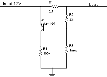
Is the following PNP transistor going to overheat in this circuit (attached)?

The PNP transistor is put there so as to provide a low output on its collector if the load ever goes open.
However, the PNP is just a CPH3105 type, and is in a SOT23 package, and is on a minimal footprint on the PCB, with no cooling copper added to any of its pads.
This PNP is dissipating 175mW (Ieb * Veb)

PNP circuit.jpg

CPH3105 PNP transistor datasheet:
https://www.onsemi.com/pub_link/Collateral/EN6084-D.PDF
 
Last edited by a moderator:

Virtually all your load current goes through the EB junction. Check whether the transistor can handle this. If your load is a filament lamp, you may fry the transistor because of the inrush current for the lamp. When the load has a large input capacitor, you will fry the transistor also.
 
  • Like
Reactions: treez

    T

    Points: 2
    Helpful Answer Positive Rating
The problem is that with a load current of 175 mA, there will be a voltage drop of .175 X 100 = 17.5 volts across R2. This is clearly impossible!!. Changing R2 to 5 ohms will give a drop of 5. X .175 = .875V. Put a 1K resistor in series with the feed to the base to limit the base current. You need 12V/100K = 120 micro amps of collector current or one micro amp of base current.
Frank
 
  • Like
Reactions: duzuike and treez

    T

    Points: 2
    Helpful Answer Positive Rating

    duzuike

    Points: 2
    Helpful Answer Positive Rating
Thanks
WimRFP:...good point, there *is* a 22uF electrolytic capacitor on the base of the PNP....My apologies, I have added it into the schematic now in the top post.

Chuckey:
The CPH3105 datasheet says that the CPH3105 can handle up to 600mA through its base_emitter junction

(In case anyone is interested, the actual load is 2 LEDs being driven by a LDU0830S350 module)

This circuit has already been implemented and is currently used in a car (just been installed)...ive been asked to check the schematic, and this is one of the points id like to check.
 

I would try something like this:

4491122300_1391092441.png


R2 gives some pre-bias so that 0.5V across R1 is sufficient. R2 also protects the transistor against inrush issues.
 
  • Like
Reactions: treez

    T

    Points: 2
    Helpful Answer Positive Rating
Thanks WimRFP, though in your schematic, will your Q1 turn OFF if the load goes open?
...I mean, it all depends on the hfe, which is widely variable....i dont think I can gaurantee that your Q1 will turn off if Q1 is a high hfe device?

I mean, I see that your 1 meg does limit the base current when the load goes open....but can it always limit it enough?
...and also, if the 1Meg was made of even higher value, then the PNP would never turn ON in the first place when the load was present.
 
Last edited by a moderator:

When you remove the load, Veb will be 12*33/(33+1000) = 0.38V. At about room temperature a general purpose transistor (BC557B) will be off.

With 0.175A, Veb will be:

0.38+2.7*0.175 = 0.85, and then the transistor will be "on".

To get 12V across 100k, you need 120uA, at this current a general purpose transistor has hfe>100, so the base current will be < 1.2uA. The bias current through the 1 MOhm resistor is about 12 uA, so sufficient to drive the transistor. Do you have a simulator? If so , just try it and play with hfe and temperature.

When the 100 kOhm is less in the actual application, you may reduce R2 and R3 (keep same ratio).

The "pre-bias" helps to reduce the dissipation in R1 (now 80mW), and the voltage drop is less. You can just use BC557B (or similar general purpose type).

If the circuit needs to work over very large temperature range, you need a second transistor for temperature compensation.

You may add a capacitor across BE to avoid false triggering due to transient phenomena (EMC issues).
 
  • Like
Reactions: treez

    T

    Points: 2
    Helpful Answer Positive Rating
Thanks
But ill need to re-check your calculations with the automotive input voltage range of 10 to 16V, and ensure that no false tripping occurs.

Anyway, your circuit uses more components than the original circuit (in the top post), so may I ask what's so wrong with the circuit in the top post.?
 

Automotive range (including temperature): you can't use my simple circuit, then you need a second transistor that will almost eliminate voltage and temperature influence.

You will fry your transistor circuit when connecting loads with significant inrush current as the inrush current has to go through the base.

If you still like the simple approach: increase R1 to say 4.7 Ohms and remove the 1 Mohm resistor. You can go from 33 kOhms to say 3.3 kOhms. Now your transistor will not see inrush current. Of course the 4.7 Ohms resistor needs to handle inrush current.

Other option is rigorous testing of your circuit using a margin on top of real world current waveforms (including transients). When this is for a high volume application, this approach can be cost effective.
 
Last edited:
  • Like
Reactions: treez

    T

    Points: 2
    Helpful Answer Positive Rating
You will fry your transistor circuit when connecting loads with significant inrush current as the inrush current has to go through the base.
The only inrush is that inrush into the 22uF capacitor, surely that won't fry the PNP in the schematic of the top post?
 

If the input power (left side of your circuit) arrives via a switch (or some other fast switching electronic device) from a car battery, you can have inrush current in the 10 A range (of course for short duration). If this can happen in real world, I would not use the circuit without rigorous evaluation/testing. If somebody can't comfirm its fine, or there is no time or funding for such testing, I would go for another circuit.

BC857 cost about 0.04USD, your transistor is about 0.19USD (3K price from Onsemi).
 
  • Like
Reactions: treez

    T

    Points: 2
    Helpful Answer Positive Rating
10A inrush (at least) happens in bridge diodes of SMPS every time an offline SMPS is switched ON.....are you saying that in this case, because the inrush is going through the "emitter_base diode" of a PNP BJT , that somehow this diode is more sensitive to inrush, and may be damaged?
 

Your are right, the inrush current goes through the base connection of the transistor.

The base current is a lateral current. As the base is relatively thin (to get usefull hfe), it has more resistance, hence more I^2*R loss. The emitter current that becomes the collector current passes the base region over its shortest path (the base thickness), and the largest area. So for the normal emitter to collector current, the base resistance is extremely low.
 
  • Like
Reactions: treez

    T

    Points: 2
    Helpful Answer Positive Rating
the CPH3105 datasheet (linked in the top post), states that Ib can be up to 600mA.....so do you think that they are referring to 600mA only for a short interval of time, as in 'switching' operation? (the datasheet does say this BJT is for "switching" operation.)
What voltage do you think will be across the Vbe junction in the circuit of the top post...?
 

I think it will be less then 1 V at 0.175A, as Vbesat < 1V at Ic=5A with forced hfe = 50 (that means Ib = 100 mA). When you only have Ib, you don't have the voltage drop across Ree' because of the collector current. So you can have some additional voltage drop across Rbb' (as you use 0.175 A instead of 0.1 A).

I also saw Ib = 600mA (without "Pulse" or other time limitation), and the note below it (regarding reliability). As long as you don't know actual peak currents during the life of your circuit, you can't say anything about the reliability. When it is used from vehicle onboard voltage, voltage transients at the input will cause peak currents because of the 22uF capacitor in your circuit. I did some automotive redesign and joined automotive EMC testing. Pulses during EMC testing have low impedance and therefore can generate large current transients if you don't stop them from reaching your input.

Is this just for a single (hobby) project, or for actual high volume production (as you mentioned number of components in #8)?

You need to add a diode parallel to the 100 Ohms resistor in posting #1 (anode on right side). When the input voltage drops suddenly to a low value, the EB diode will be reversed biased (because of the charge in the capacitor). Transistor BE junctions breaks down around 7V.
 
Last edited:
  • Like
Reactions: treez

    T

    Points: 2
    Helpful Answer Positive Rating
I would prefer a low ohmic shunt < 1 ohm and a degenerated current mirror (e.g. BCV62) as sense amplifier.
 
  • Like
Reactions: WimRFP and treez

    T

    Points: 2
    Helpful Answer Positive Rating

    WimRFP

    Points: 2
    Helpful Answer Positive Rating
@FVM: I agree with you, especially because of low-cost matched pairs such as BCM 857. You can go below 100mV across the sensing resistor.
 
  • Like
Reactions: treez

    T

    Points: 2
    Helpful Answer Positive Rating
this is for a car reverse, fog and drl lights (LED)

I would prefer a low ohmic shunt < 1 ohm and a degenerated current mirror (e.g. BCV62) as sense amplifier.
..is there any reason why you don't favour the circuit of the top post?...is it the dissipation in the sot23 that troubles you about it?

I think it will be less then 1 V at 0.175A, as Vbesat < 1V at Ic=5A with forced hfe = 50 (that means Ib = 100 mA). When you only have Ib, you don't have the voltage drop across Ree' because of the collector current. So you can have some additional voltage drop across Rbb' (as you use 0.175 A instead of 0.1 A).
...thanks, though previously you said that the BE junction was high resistance, and so the volt drop going through it would be higher?
 
Last edited by a moderator:

...thanks, though previously you said that the BE junction was high resistance, and so the volt drop going through it would be higher?
He's suggesting that 75mA may cause less voltage drop than 5A, even though it's going through a higher resistance.
 

The base current is a lateral current. As the base is relatively thin (to get usefull hfe), it has more resistance, hence more I^2*R loss
...the above were the kindly donated words from WimRFP.....clearly this infers that the BE junction is a high reistance region.

WimRFP's other kindly donated words were as follows...
I think it will be less then 1 V at 0.175A, as Vbesat < 1V at Ic=5A with forced hfe = 50 (that means Ib = 100 mA). When you only have Ib, you don't have the voltage drop across Ree' because of the collector current. So you can have some additional voltage drop across Rbb' (as you use 0.175 A instead of 0.1 A).

...I though, disagree here, the CPH3105 datasheet says nothing relevant to the "weird", bizarre PNP connection of my top post.....I am sorry, but control current goes BE, power current goes CE...that is the only situation that the datasheet will discuss.....so inferring what would happen when one has 50 times more ib than ic is the stuff of some other bizarre universe.

I note that FvM has said that he would prefer an alternative to my top post, even though FvM's alternate method is using slightly more components....at least I believe so?

Can you imagine what the analog designers at onsemi.com would say if we told them that we wished to use their CPH3105 PNP by putting 175mA from E to B, and just a few microamps from E to C?....they would say we were mad, and implore that the datasheet just doesn't account for such bizarre connection methodology.....In 1956, Bardeen, Shockley & Brattain didn't invent the BJT so it could be used with power current flowing E to B, then virtually no CE current.
 

Status
Not open for further replies.

Part and Inventory Search

Welcome to EDABoard.com

Sponsor

Back
Top