Continue to Site

Welcome to EDAboard.com

Welcome to our site! EDAboard.com is an international Electronics Discussion Forum focused on EDA software, circuits, schematics, books, theory, papers, asic, pld, 8051, DSP, Network, RF, Analog Design, PCB, Service Manuals... and a whole lot more! To participate you need to register. Registration is free. Click here to register now.

[CST] Mesh settings for Nano antennas??

Status
Not open for further replies.

kela3kela

Full Member level 4
Joined
Apr 30, 2009
Messages
191
Helped
5
Reputation
10
Reaction score
5
Trophy points
1,298
Activity points
2,502
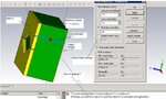
Im simulating a dual vivaldi nantenna in CST MWS. The design is shown below with the error mentioned in terms of Mesh settings alongside the attached paper.

The frequency range is 0.7-3.5 GHz.
THe substrate dimension is 2x2 um.

Could someone plz tell me what mesh settings should i use when working with nano antennas???
Awaiting replies,

Regards
 

Attachments

  • Vivaldi antenna.pdf
    207 KB · Views: 93
  • Nantenna.jpg
    Nantenna.jpg
    71.4 KB · Views: 96

You have to forget about microwave band (0.7-3.5 GHz). You have a 2x2 um structure which is around 1/100000 of lambda, no software can mesh it and the structure neither resonate nor radiate there. You have to go to the optical (or nearby) wavelengths where the mentioned paper is using!
Regards,
Hadi
 

Thnx for the reply.

So according to the paper, the wavelength they r using is from 0.7-3.5 um which is in THz frequency. The software is CST but in Frequency domain..feeding with parallel wave guide.
I'll try with the above mentioned parameters and see what happens...
 

Ok...I redid the simulation as per papers suggestions but i now im getting the following error...Can you help??

This time its only one substrate and Gold on top of it, no ground plane and excitation is between the gap of Gold plates via discrete ports....

Untitled.jpg
 

This photo means that you meshes should be even finer in order to recognize the port you have defined. For the moment the gap you have put for the port is seen like the junction between two metals. for instance put the mesh density 20 "lines per wavelength".
 

Tried 20 lines per wavelength but Still same error.... :(
 

I'm still pretty sure about it! :| I suggest either to increase it more (30 line i.e) or to widen the port's gap a bit more. I looks really small. :wink:
 
Cant widen the gaps as it optimised as per paper values..Ill try mesh of 200 and c what happens...
 

Im still getting errors...
@hadi-Alk: Brother if I send u the CST file, could u simulate it for me??
 
Last edited:

What is the version of your CST file, kela?
 

It is solved,
Actually it is just enough to change your boundary setting from Et=0 (PEC) to open add space or open. In fact, you case was quite vague, because you ports are that boundary and touching the PEC you defined at the boundary. Now you can solve it even with 10 meshes per line, just change the boundary condition :). Sorry for delay
 
Thnx...If possible could u upload the solved CST file..It would b helpful...
Regards
 

Hi again,
You can find it here:
**broken link removed**
 
Status
Not open for further replies.

Similar threads

Part and Inventory Search

Welcome to EDABoard.com

Sponsor

Back
Top