Continue to Site

Welcome to EDAboard.com

Welcome to our site! EDAboard.com is an international Electronics Discussion Forum focused on EDA software, circuits, schematics, books, theory, papers, asic, pld, 8051, DSP, Network, RF, Analog Design, PCB, Service Manuals... and a whole lot more! To participate you need to register. Registration is free. Click here to register now.

Stable amplitude ultra wideband oscillator positive supply conversion

Status
Not open for further replies.

neazoi

Advanced Member level 6
Joined
Jan 5, 2008
Messages
4,123
Helped
13
Reputation
26
Reaction score
15
Trophy points
1,318
Location
Greece
Activity points
36,955
Hello,
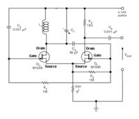
I would like to experiment with this oscillator **broken link removed**
The final circuit is shown here **broken link removed**

It requires a negative voltage. Is there any way I can convert it to a positive voltage?

Virtual ground systems are not good, since the -V is connected to the PSU GND. Capacitor charge pumps may be a solution, but maybe it would be easier to convert it to require a positive voltage?
 

You can, mirror/flip the circuit around the x-axis. -10V becomes the ground and the ground connection becomes the + 10V.

Make sure you have good AC decoupling from the new +10V connection to the new ground connection. Very likely you know that allready as this isn't your first RF circuit...
 

You can, mirror/flip the circuit around the x-axis. -10V becomes the ground and the ground connection becomes the + 10V.

Make sure you have good AC decoupling from the new +10V connection to the new ground connection. Very likely you know that allready as this isn't your first RF circuit...

You mean connecting the GND of the PSU to the -V in the circuit and the +V of the PSU to the GND of the circuit? That is mirroring, it would work, but then I could not use the PSU for the following buffer amplifiers as they will require another isolated PSU.
 

@Godfreyl: Thanks for redrawing the circuit.

@Neazoi: Godfreyl circuit is fine, it does work the same as your negative supply version.

As mentioned before, make sure your have good decoupling from 10V to ground as noise in the 10V will add to the output (via c3). Your decoupling should also work for low frequencies as otherwise you will get additional phase/frequency noise.

I worry that with this version you lose the advantage of grounding one end of the LC. This could lead to frequency instability. I was refering to a version that grounds the LC but have positive +V. Maybe using P channel fets instead of N
 

There are very few PJFET and effectively no RF-amplifier type available.

The only point where the ground referred drain circuit really matters is the output load resistor. At this place, good bypassing is necessary.
 

@Neazoi: As long as you have good decoupling from the positive supply plane to the ground plane, there is no difference between the circuits. Just make a large size copper area/patch that serves as the 10V supply. Make it so large that you can easy solder all components to it. Make sure you decouple this to the surrounding ground copper area with several SMD capacitors at all sides of the 10V plane. many smaller ones is better then some large value ones.

By doing this, you make a copper patch that is really ground for RF, but is at +10V DC level.
 

there are circuits that do that:
http://pdf.datasheetcatalog.com/datasheet/zetexsemiconductors/znbg4000.pdf

If u search around, there are ICs that also only do the negative gate bias part.


A simple capacitor pump could be used no need for such ICs. A capacitor charge pump will also provide a common ground for the GND of the PSU and the charge pump GND. So this is the obvious solution.

I wondered if the schematic could be converted to avoid the -v converter at all.
 

To be honest, based on your info, I don't see any need for a charge pump to generate a negative supply voltage, as the positive supply version is as good as the negative supply version. In addition, you are free of switching transients that may result in phase/frequency noise.
 

Status
Not open for further replies.

Part and Inventory Search

Welcome to EDABoard.com

Sponsor

Back
Top