Continue to Site

Welcome to EDAboard.com

Welcome to our site! EDAboard.com is an international Electronics Discussion Forum focused on EDA software, circuits, schematics, books, theory, papers, asic, pld, 8051, DSP, Network, RF, Analog Design, PCB, Service Manuals... and a whole lot more! To participate you need to register. Registration is free. Click here to register now.

500VA sine wave inverter , problem in HBridge and filter designing

Status
Not open for further replies.
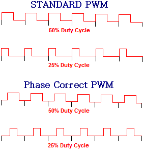
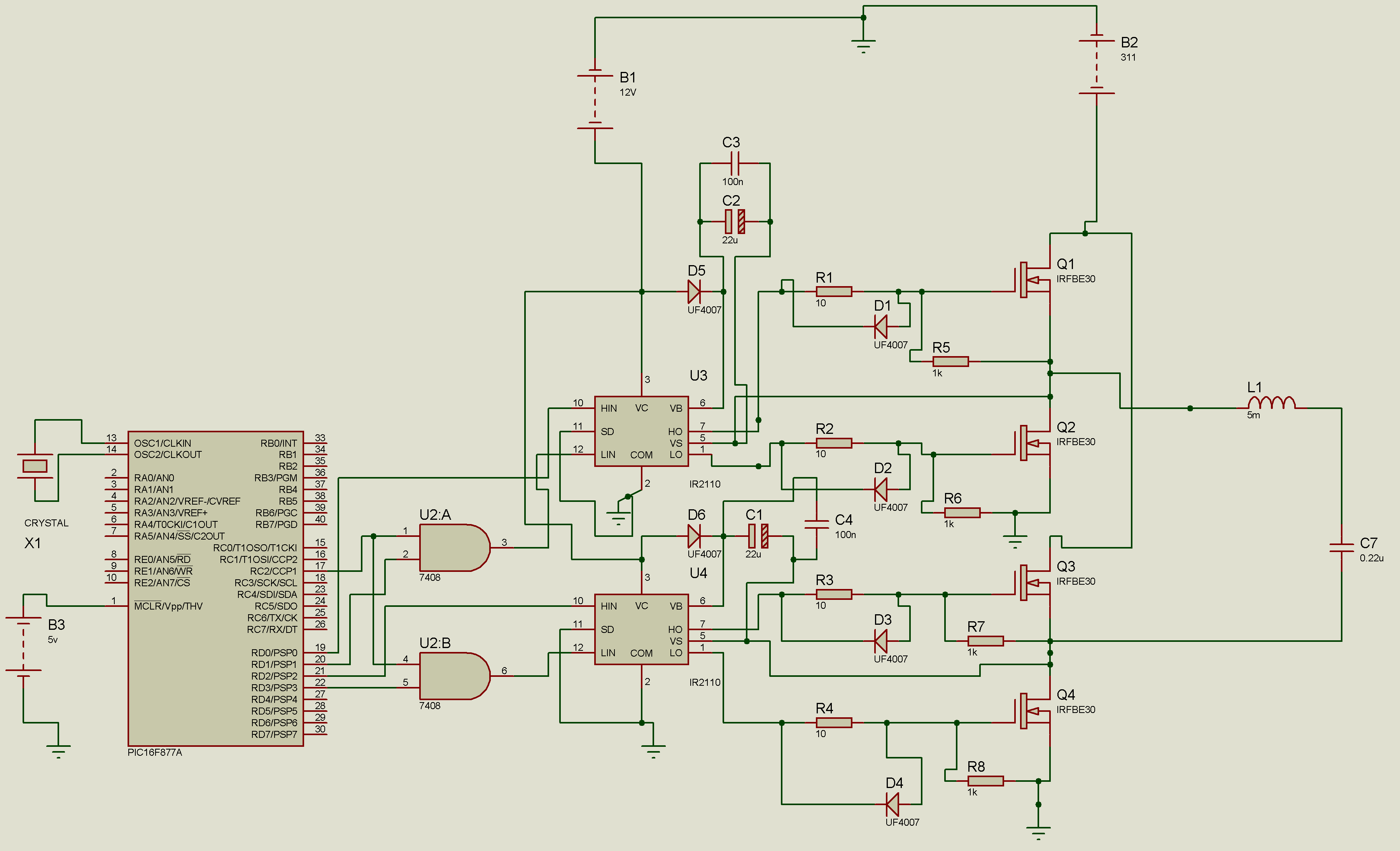
FvM , if i use AND gate to utilize single pwm port as double one. Will it work?
As in unipolar spwm one has to drive switch S1 and S3 (diagonally)by a spwm signal and after that S2 and S4 are driven by another spwm signal which is 180 degree phase shifted..in between a small deadtime is provided..so i wanna ask if i hve only single pwm port and with the help of AND gate will it be possible to utilzee it as two pwm ports ...?
 

Bawa what did you use to drive the H bridge. is it IR 2110
 

You need at least two independent PWM outputs (for the "180 degree phase shifted" signals) and extenal deadtime generation.
 
You need at least two independent PWM outputs (for the "180 degree phase shifted" signals) and extenal deadtime generation.
FVM is right you need two different outputs from MCU. Another most important point is while one arm of H bridge gets Modulated SPWM signal other arm should be held off by a 50Hz low signal for proper operation
regards ani
 
can u tell me any 8bit microcontroller which has 2 independent PWM outputs?
 

Another most important point is while one arm of H bridge gets Modulated SPWM signal other arm should be held off by a 50Hz low signal for proper operation.
You will get all your info from this link https://www.edaboard.com/blog/1800/
You are talking about the simplified PWM method that's already used in BaWa's original project. Now he's asking about a different modulation method which requires two independent, center aligned PWM outputs.

The present question is about µCs supporting center aligned PWM, two or better four outputs with internal dead time generation. As fas as I'm aware of, it's not offered by Microchips ECCP units.
 
can u tell me any 8bit microcontroller which has 2 independent PWM outputs?
Some of 8bit microchip microcontroller having 2 PWMs
PIC16F1825,PIC16F1827,PIC16F1828,PIC16F1829,PIC16F1847,PIC16F707,PIC16F722,PIC16F722A,PIC16F723,PIC16F723A,PIC16F724,PIC16F726,PIC16F727,PIC16F73,PIC16F74,PIC16F76,PIC16F77,PIC16F882,PIC16F883,PIC16F884,PIC16F886,PIC16F887,PIC16F914,PIC16F917
 

These processors have multiple PWM units, but they don't support center aligned modulation without akward programming.
 

FvM , do you know anyother 8bit processor which can solve my purpose?
is arduino is capable of generating unipolar spwm?
i want to learn more about unipolar spwm ,can u suggest any link or ebook?
 

Atmel's mcus, for example Atmega8 has option for phase corrected {center aligned) ouputs.

6316342500_1380702065.gif


Have a look on these pages.

https://www.avrfreaks.net/index.php?name=PNphpBB2&file=printview&t=68302

**broken link removed**

It is quite a long time, you are stuck with this project.
if you provide full detail, I shall replicate and try to understand what is going wrong.
 
ya ALERTLINKS, i hve been working on this project snce 11 months, i am very close to output,
i m going to provide u complete details,
inverter rating is 400VA ,230volts, 50hz.
1) i am using BIPOLAR SPWM generated by microcontroller. below is the image
6443312500_1372268332.png

also i have provided proper dead time
9393161100_1372268469.png


below is my HBRIDGE circuit
3809237300_1372268536.png

as suggested by FvM, i've also changed gate resistor to 47 ohms, and gate to source resistor to 4.7k, also bootstrap capacitor is 47uf.
one thing i didn't implemented was the DC link capacitor near hbridge, although i have used DC link capacitor but connecting was approx 1/2 feet away from my hbridge circuit.
now the problem is , when i test my circuit at low voltage (32 volts ), i get a nice sine wave in the output,
as i connect my high voltage DC bus to hbridge and filter not connected, my circuit works fine , i also tested the 100 watt bulb(resistive).
but as i connect filter to the h bridge , my hbridge mosfets get damage, also the mosfet bank of DC DC stage also gets damage.
, now what m thinking is , may be the problem is due to inductive load (filter). as FvM said the problem is due to slow body diode conduction . and to overcome this problem i have to use UNIPOLAR SPWM.
now i want to generate UNIPOLAR SPWM from any microcontroller, i want to learn this. and i have to complete my design . so if u can send me any link of UNIPOLAR SPWM and how to generate it from mcu. it will be very helpful.
Hi ,
It is better that you provide dead time in the channel A and C signals instead of going to change the entire software and hardware. Once you provide deadtime in RD1 and RD3 signals comming from PIC Dead Time will be there independent of Whatsoever signals You have in the other two arms.
I strongly believe that the problem is with the filter since the circuit is working fine with 310V DC bus with 100W bulb. You may try adding a small inductive load along with the 100w bulb incircuit without filter, I think it will also work fine.
Regards ani
 
I agree with Picgak. This design is practical. You should complete it first. To replicate your system front and back of your boards and hex code will be required. I suspect the cause of malfunction is more, the RF interference generated by the inductor rather than any other issue, generated due to improper layout.
I found these documnts of your interest,

**broken link removed**

https://digitalcommons.calpoly.edu/cgi/viewcontent.cgi?article=1210&context=eesp

Dead-time between RD1 and RD3 is not important as both hi-side FETs are off. I hink you are you following this the blog.
https://tahmidmc.blogspot.com/2013/02/generation-of-sine-wave-without-eccp_16.html

I'll try to assemble it.
 
Last edited:
Mixing the discussion about problems of the original design with the unipolar SPWM related question seems to confuse the discussion. I have commented the former point in detail and don't see a reason to repeat what's been already said.

I agree with the statements saying that an inverter according to the original schematic should work with suitable circuit layout.

I also keep my opinion that changing the design to synchronous switching, which must not necessarily use the classical unipolar SPWM scheme, can avoid the problems involved with reverse recovery of slow MOSFET body diodes.

Referring to the latest question
Will dspic be able to generate unipolar spwm?
dsPIC30F Family Reference Manual has a paragraph "Center Aligned PWM", so it's obviously designed to generate it. You have to review the individual datasheets to find out which chips are implementing the feature.
 
below is my hbridge circuit, i have designed it using eagle
20131004_000143.jpg
20131004_000220.jpg
u can see some bad connection near my microcontroller , i hve put a jumper over there , and the circuit is working fine whrn i am using 12vdc as input to hbridge.
i didn't put filter on the same pcb, i hve attached my filter using wires , and i was getting sine wave at low voltage test. below is my filter image
20130912_200442.jpg
the bulb in the image is acting as a damper ,which is connected in series with filter capacitor. also i have tested my circuit without bulb .

the DC bus capacitor were also not in the HBRIDGE circuit board , i have put those capacitors on another veroboard, and connect them to hbridge using 15cm copper wire. below is the image of dc bus capacitor, 100uf each were used
20131004_000449.jpg
also the dc bus ceramic capacitors were on my DC DC converter board . u can see it below
20130912_200531.jpg
this above circuit is my dc dc stage , and it was working fine, i have tested it using 200 watt bulb,, also dc bus is regulated. the torroid u can see is used for filtering the dc.
the ceramic capacitor is placed behind that torroid so its not visible.

below is my complete setup image
20130912_200659.jpg

i have tried it again n again but didn't get success, this was my 32th PCB, i have made. now as suggested by FvM , i am thinking to implement UNIPOLAR SPWM.

FvM , if use a small torroid transformer to convert edge alligned pwm to center aligned pwm, will it work ,, i mean if i use my 8bit MCU to generate spwm (which i am currently generating). now if i make a small torroid center tape transformer to get that spwm as well as the compliment of that spwm at the output of the torroidal transformer , will this method work?
 
Last edited:

I don't understand at first sight what a transformer should do to generate center alligned PWM.

If I remember right, the necessity of bus capacitors placed directly at the H-bridge transistors has been has been stated by several contributors in your previous thread.

Apart from this problem, I doubt that the board has sufficient ground wiring.
 
FvM. I hve also made a new layout .in which i have put the capacitors near the h bridge .
FvM said:
Apart from this problem, I doubt that the board has sufficient ground wiring
Plz expain this ..i didn't get this..
 

Status
Not open for further replies.

Similar threads

Part and Inventory Search

Welcome to EDABoard.com

Sponsor

Back
Top