msdarvishi
Full Member level 4
Dear colleagues,
Hello,
I am trying to find the response of a set of cascaded inverters into a pass-transistor. First, I put "one" inverter (configured of an NMOS & PMOS) and connected it into the pass-transistor. The response was significantly and the transistors in inverter were in regions 0 Tcut-off) or 1 (triode). Second, I put "two" inverters connected into the pass-transistor and I found that the pass-transistor went into region 3 (saturate) and the regions of first inverter were 2 for PMOS and 1 for NMOS and 0 & 1 for the second inverter ...!!
Anybody could help me to understand this phenimenon?
Thanks
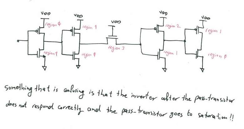