Welcome to our site! EDAboard.com is an international Electronics Discussion Forum focused on EDA software, circuits, schematics, books, theory, papers, asic, pld, 8051, DSP, Network, RF, Analog Design, PCB, Service Manuals... and a whole lot more! To participate you need to register. Registration is free. Click here to register now.
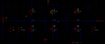
I was assigned to design chain according to 74CH04 at tempt 25C. Is this one correct? Do I need to improve the schematic? Tq for any help handsome guys .
It looks as though it might be that simple. It wasn't assigned as a trick question, by any chance?
Could the CH series be different from other families?
Was there any specific characteristic the inverter should have?
Delayed transition? Static CMOS inverter? Saturated load digital inverter? Class A arrangement using one resistor and one mosfet? (Looking at the Wikipedia article.)
first you dont have to add an excitation for your oscillator ( vin have to be omitted) ( the oscillator oscillates by itself !!)
second you have to set an initial condition for your oscillator to help the simulator converge
Simulation->Convergence Aids->Initial Condition
otherwise you have an excellent book from Razavi "Digital microelectronics circuits"
Hi again, I need to determine VOH and VOL for the circuit on first post, and fir simulate it we need to add current source, VOH= negative value current and VOL=positive value current. Can anyone plot me where should I place current source to circuit respectively for both VOL and VOH?
This site uses cookies to help personalise content, tailor your experience and to keep you logged in if you register.
By continuing to use this site, you are consenting to our use of cookies.
 .
.