Continue to Site

Welcome to EDAboard.com

Welcome to our site! EDAboard.com is an international Electronics Discussion Forum focused on EDA software, circuits, schematics, books, theory, papers, asic, pld, 8051, DSP, Network, RF, Analog Design, PCB, Service Manuals... and a whole lot more! To participate you need to register. Registration is free. Click here to register now.

Opam circuit analysis problem

Status
Not open for further replies.

anhnha

Full Member level 6
Joined
Mar 8, 2012
Messages
322
Helped
4
Reputation
8
Reaction score
4
Trophy points
1,298
Activity points
3,684
Hi everyone,
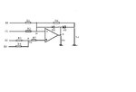
Below is is part of solution of my problem, but there are some things make me confuse.
The solution is:

Eo=Up= E2. R4/(R3+R4) + E3. R3/(R3+R4)
If U1< Eo => Un< Up => Ud= Up - Un > 0 => Ua> 0
then D1 is conducted and D2 is not conducted.
If U1> Eo => Un> Up => Ud= Up - Un < 0 => Ua< 0
then D1 is not conducted and D2 is conducted.
What make me confuse is that
I think in order to know a diode is conducted or not we have to know the bias of diode or the voltage is appy to diode, we have to know both the voltage sides of diode.
In the solution why we can conclude when U1< Eo then Un < Up (Why Un is not equal to Up).
Why we can conclude when Ua <0 then D1 is not conducted and D2 is conducted.
Thanks a lot.
 

Attachments

  • Amplifier.JPG
    Amplifier.JPG
    23.6 KB · Views: 69

anhnha,

What is the problem you are trying to solve? All I see is a drawing and a bunch of statements and equations that have no relevancy to each other. A problem well defined is a problem half solved.

Ratch
 

anhnha,

What is the problem you are trying to solve? All I see is a drawing and a bunch of statements and equations that have no relevancy to each other. A problem well defined is a problem half solved.

Ratch
Thanks for replying.
My problem is that the bias of diodes when U1 (op amp input Voltage ) vary.For example:
Why U1 < Eo then D1 is conducted and D2 is not conducted?
Why U1 > Eo then D1 is not conducted and D2 is conducted?
where Eo is the voltage at P pin of op amp, and its value:Eo=Up= E2. R4/(R3+R4) + E3. R3/(R3+R4)
Could you help me explain it?
 

- 1) This Op Amp provides differential gain relative to a bias point assisted with input U1 which has more influence with a low value on summing point N and must match the summing point P on the + side to satisfy the 0V different on +/- input. Ideally this serves to balance the offsets in E1 to match E2&E3 initial levels.(factored by the loss/gain R ratios.
- 2) THe 2 diodes serve 1 purposes to make a half-wave rectifier Amp. For negative inputs on E1 relative to E2,E3 the output is positive with >100dB gain until D1 conducts and reduces inverting gain, lets call it Av-, to zero. E2,E3 offset remains at unity gain to output Ua, (relative to U1 bias point) So D1 rectifies negative inputs on E1

or in other words, OpAmp rectifies more positive inputs on E2,E3 summing point, P, the Positive input to output.

- 3) for negative swings on the output, Ua, D2, conducts with very little offset since the OA has a gain of>100dB and that is a much lower resistance than R6, so the signal gain from E1 to Ua is -R6/R1

So in short, (no pun intended) D1 blocks positive signals on P relative to N input sides and D2 selects R6 as the fixed gain ratio for negative signals on the P side relative to N.
So in short a negative precision half-wave rectifier with gain controlled by R6 and bias point set by U1. or E1 visa versa.
U2 is not used as a useful output.


That's it. After a while you dont need to do the equations and you can see the gain from familiarity.
 
  • Like
Reactions: anhnha

    V

    Points: 2
    Helpful Answer Positive Rating

    anhnha

    Points: 2
    Helpful Answer Positive Rating
Isn't his output, Ua, going to ground or what is that symbol suppose to indicate?
 

Status
Not open for further replies.

Similar threads

Part and Inventory Search

Welcome to EDABoard.com

Sponsor

Back
Top