Continue to Site

Welcome to EDAboard.com

Welcome to our site! EDAboard.com is an international Electronics Discussion Forum focused on EDA software, circuits, schematics, books, theory, papers, asic, pld, 8051, DSP, Network, RF, Analog Design, PCB, Service Manuals... and a whole lot more! To participate you need to register. Registration is free. Click here to register now.

Microstrip layout question

Status
Not open for further replies.

EEPC

Newbie level 6
Joined
Oct 8, 2010
Messages
14
Helped
0
Reputation
0
Reaction score
0
Trophy points
1,281
Activity points
1,459
Hi guys,

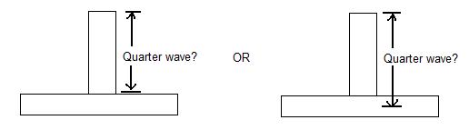
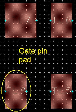
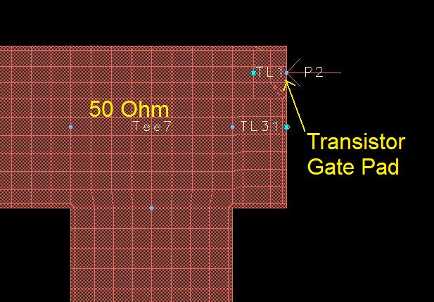
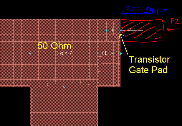
I have a question about doing layout in microstrip. If I have a 50 ohm line that I want to attach to the gate/drain/source pins of a transistor package, can I just solder the transistor on a corner of the 50 ohm line? Or do I have to create a short length of line with width that matches the width of the package pins and then connect the narrow line to my main 50 ohm line? This seems to create severe junction effects that affect overall performance, but I'm not sure what the effect of attaching the pins at one corner of the 50 ohm line would be. This should produce less junction effects, but then the pins can't be aligned in the center of the microstrip line.

What is typically done in layout for connecting transistor pins to input/output microstrip lines?

Thank you!
 

The usually practice to connect a wider lead transistor to a narrow width 50 ohm microstrip is the same as you guessed: create a wider enough pad to solder the lead on it and connect 50 ohm line to the pad. As you're already aware, this will cause some discontinuity issue. However most of them can be solved by correct matching. Solder the lead to the corner listens not a good idea. But since no picture about what your circuit like so it maybe work also. Try to use EM simulation software to check your design before release your PCB whatever solution you choose.
 
Like pewang mentioned, avoid "stepping down" the transmission line to make a small pad for the transistor, as it will cause discontinuities and hurt your performance. I also agree with not soldering the part to the corner of the 50 ohm line. If you can, run the 50 ohm microstrip all the way under the pin of the device, and solder the part down on the center of the 50 ohm microstrip. If you wind up with 50 ohm lines that will run into each other, selectively trim down the traces until they all fit under the device.

For a good verification step, pewang's suggestion for simulation with an EM solver is also my recommendation.
 
  • Like
Reactions: EEPC

    EEPC

    Points: 2
    Helpful Answer Positive Rating
Thanks pewang and enjunear for the help! In my case the transistor pads are much smaller than my 50 ohm lines. For example, my 50 ohm lines are ~3 mm in width and the transistor pin pads range from ~0.6-1.5 mm in width, so I definitely cannot just align all the pins at the center of the 50 ohm lines. Enjunear, do you mean I should just trim the width of the 50 ohm lines in the vicinity of the transistor pads to get them all to fit? How should this be done without "stepping down" (making narrower) the line widths? With tapers?

I will also definitely run EM simulation in Momentum to verify.

One quick question that's unrelated: let's say I have two series length of 50 ohm microstrip lines and I want to attach a quarter-wave stub in between them. In ADS when I do layout I add the MTEE component at the junction. This basically gives me a square and appends each microstrip line to one side of the square. This essentially increases the length of the line, right? And I have to reduce the original line lengths? Also, does the quarter wave stub also need to be reduced in length with the addition of the MTEE? I'm slightly confused about where the quarter-wave length is defined from, the edge or center of the main lines? This might not make sense so I drew a quick picture of my question that I attached:


Enjunear, do you mean I should just trim the width of the 50 ohm lines in the vicinity of the transistor pads to get them all to fit? How should this be done without "stepping down" (making narrower) the line widths? With tapers?

Simply minimize the amount of "damage" you do to your 50 ohm lines. The longer the microstrip looks like a 50 ohm line as it comes up the part, the better. How you implement that depends on the package of the device and how your traces have to be routed around the device.


One quick question that's unrelated: let's say I have two series length of 50 ohm microstrip lines and I want to attach a quarter-wave stub in between them. In ADS when I do layout I add the MTEE component at the junction. This basically gives me a square and appends each microstrip line to one side of the square. This essentially increases the length of the line, right? And I have to reduce the original line lengths? Also, does the quarter wave stub also need to be reduced in length with the addition of the MTEE? I'm slightly confused about where the quarter-wave length is defined from, the edge or center of the main lines? This might not make sense so I drew a quick picture of my question that I attached:


In a true theoretical microstrip-based analysis, the quarterwave stub would be defined like the left-hand image (in ADS, the length of the MLIN would equal the length of the stub). However, in reality, each bit of copper will interact with all of the other bits of copper. So, in practical application, you'll find that the length of your quarterwave stub will be closer to the right-hand image. If you tune the circuit using the schematic components, you'll get the "textbook" answer. When you tune the circuit using Momentum (which meshes and solves for all of the metal-metal interactions), you'll get a slightly different answer. However, the Momentum answer will be closer to what it acts like in the real world.

Most designers start with a schematic-based design for quick simulations (closed form solutions, quick for a CPU to crunch those equations). When you want to fabricate a design, you then port it to the Layout window and start using Momentum (or any other EM solver) to figure out how the artwork will work in real life, with all of the interactions and couplings being taken into account.
 

Hi, EEPC
Your first question is now cleared for me. In your case, you sure can solder the lead to a coner of 50 ohm but the better solution is to use a taper transformation to adopt this width change.
For your 2nd question, firstly you need to read the MTEE model definition helper file to see where is the edge boundary of this component. From my opinion, your first drawing is good for initiated design.
 
  • Like
Reactions: EEPC

    EEPC

    Points: 2
    Helpful Answer Positive Rating
In my case the transistor pads are much smaller than my 50 ohm lines. For example, my 50 ohm lines are ~3 mm in width and the transistor pin pads range from ~0.6-1.5 mm in width, so I definitely cannot just align all the pins at the center of the 50 ohm lines.

There is a step in width between the feedline and the leads, which introduces some series L and some small shunt C.
Sometimes, this step might be included in the measured transistor data. Otherwise, you can use a step model in ADS schematic, or include the step in the EM model. If you do it in the EM model, de-embed the transitor side port to the edge, so that it includes the step effect but no extra length.
 

Thanks again guys, I've tried all the options suggested, so far it seems like putting the transistor pads at the corner of the 50 ohm line doesn't affect the performance *too* much and I should be able to get the desired results with some slight tuning. But I don't know if I'm simulating this correctly, so I attached two pics of the layout in Momentum. The first pic shows the transistor pin pads, and the second one shows that I placed the gate pad at one corner of the MLIN and added the port at that location.

9_1335555545.jpg


volker_muehlhaus, do you mean to just use a direct step transition from 50 ohm line width to the width of the transistor leads? Do you know which would produce least disturbance in performance (direct step transition, tapered transition, or directly soldering the transistor to one corner of the 50 ohm line), or does it depend on the situation?

Thanks again, this has been very helpful!
 

Rather than making your part square to the transmission line, would you get any benefit by rotating the transistor 45 degrees? That would make the gate pin stick out, which could let you get to the middle of the 50 ohm line easier.

Also, can you tell us what device you're using?

You might find it easier to play around with the artwork if you make your transistor into a component for ADS. You do this by opening a new layout drawing. Put the metal for the pins on the leads layer, maybe make it gray in color. You can also add pre-defined solder pads around the leads (on the cond layer). Next, draw a polygon (rectangle?) on the packages layer that is close to the size of the transistor package (maybe make this outline only in the Layers editor). Now save this as something like new_2N2907A_BJT_layout.dsn, etc. Now, go into a new layout window, open the the part library (the file cabinet button in the toolbar). Under Projects, select the transistor layout drawing you just created, drag and drop it into the new layout window. Now you'll have a component that looks like your device, and the pads will stay in place, relative to each other. Then you just have you worry about changing your transmission lines leading up to the device.

Beware, you still need to have metal on the cond layer to get it to simulate correctly... the leads layer polygons will just be showing you where the part will resides, unless you add it to the Momentum substrate editor as a STRIP layer, like you normally do with COND.
 

Enjunear - the device is this one:

In layout window I put down 4 MLIN components (1 gate pad, 1 drain pad, and 2 source pads) and sized them to fit the recommended PCB pad layout (these are shown in the picture I attached earlier). I tried rotating but the separation between each pad is too small and I still wouldn't be able to get the gate to the middle of the 50 ohm line. Is the way I simulated correct? I used ADS to auto-generate the layout for the input match & biasing network and then just placed the gate pad (also a MLIN) at one corner, and then defined the gate port at the center of the pad MLIN. I then meshed and simulated just the input side metal conductors with Momentum and imported this back into the schematic to do a full simulation.

The tapered line transition to the transistor leads also seems to work alright (some adjustment/tuning would be required of course), but that requires an extra length of line. The simplest option I guess would be to just use a MTEE to connect the 50 ohm line and transistor pad, but this would probably require much more adjustment/tuning in the rest of the circuit.

I haven't found any resource online that describes the optimal way to transition from 50 ohms to the much narrower pads that comes with the transistor package, so just wondering if I'm making any serious mistakes.

Thanks again for all the help.
 
Last edited:

and the second one shows that I placed the gate pad at one corner of the MLIN and added the port at that location.

I expect that Momentum will create a port/feedline over the entire width of the line, so that the step effect is missing. I had suggested a better method above.

Note that you can "draw" in Momentum layout, and don't have to auto-layout from circuit elements as you did.


volker_muehlhaus, do you mean to just use a direct step transition from 50 ohm line width to the width of the transistor leads?

That's what I've done most of the time, up to 24GHz.

Not sure if the extra accuracy from accurate modelling is really needed for your project - what is your frequency?

Your layout is somewhat more complex, so depending on frequency, it might be worth to do an accurate model in EM simulation. Unfortunately, there seems to be no STEP element with offset available in ADS to simuate this at circuit (model) level, so EM is the only way to simulate accurately.
 
Last edited:

Hi volker_muehlhaus, I tried moving the port to the center of the 50 ohm line and it did produce different results, so perhaps Momentum is able to capture the effect of attaching the transistor leads at one corner? I'm not sure how to go about de-embedding the transistor side port in ADS. I just realized now I can draw the port at any point on the layout, so I can just get rid of TL1 (shown in my picture above) and simply add the transistor side port (port 2) anywhere along the edge of the 50 ohm line? In this case does Momentum define the port along the entire edge or only at the point I drew it at?

The main frequency band of interest is 2-4 GHz range, so not too high. Given the proximity of each of the 4 transistor pads, I wouldn't be able to transition directly from the main 50 ohm line to the transistor pads, and introducing a small length of line in between affects performance too much, and I would prefer not to have to readjust/tune values too much.
 

Hi volker_muehlhaus, I tried moving the port to the center of the 50 ohm line and it did produce different results, so perhaps Momentum is able to capture the effect of attaching the transistor leads at one corner?

Based on your experiment, I would think this is true.

so I can just get rid of TL1 (shown in my picture above) and simply add the transistor side port (port 2) anywhere along the edge of the 50 ohm line? In this case does Momentum define the port along the entire edge or only at the point I drew it at?

I' not sure about that, because I use Sonnet EM where that detail (port calibration) is implemented differently.

The main frequency band of interest is 2-4 GHz range, so not too high. Given the proximity of each of the 4 transistor pads, I wouldn't be able to transition directly from the main 50 ohm line to the transistor pads, and introducing a small length of line in between affects performance too much, and I would prefer not to have to readjust/tune values too much.

Do you really expect a relevant effect of that offset/step in width at 4 GHz? My estimate is that the effect will be small, except for the source length. Additional length at the grounded source will cause trouble, but I would just use common sense to ground the source as good (short path) as possible.
 

Status
Not open for further replies.

Part and Inventory Search

Welcome to EDABoard.com

Sponsor

Back
Top