Continue to Site

Welcome to EDAboard.com

Welcome to our site! EDAboard.com is an international Electronics Discussion Forum focused on EDA software, circuits, schematics, books, theory, papers, asic, pld, 8051, DSP, Network, RF, Analog Design, PCB, Service Manuals... and a whole lot more! To participate you need to register. Registration is free. Click here to register now.

10 bit ADC noise in Circuit.

Status
Not open for further replies.

Sajjadkhan

Full Member level 5
Joined
Sep 25, 2010
Messages
307
Helped
17
Reputation
34
Reaction score
16
Trophy points
1,298
Location
Rawalpindi,Pakistan
Activity points
4,199
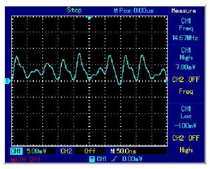
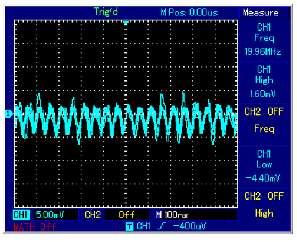
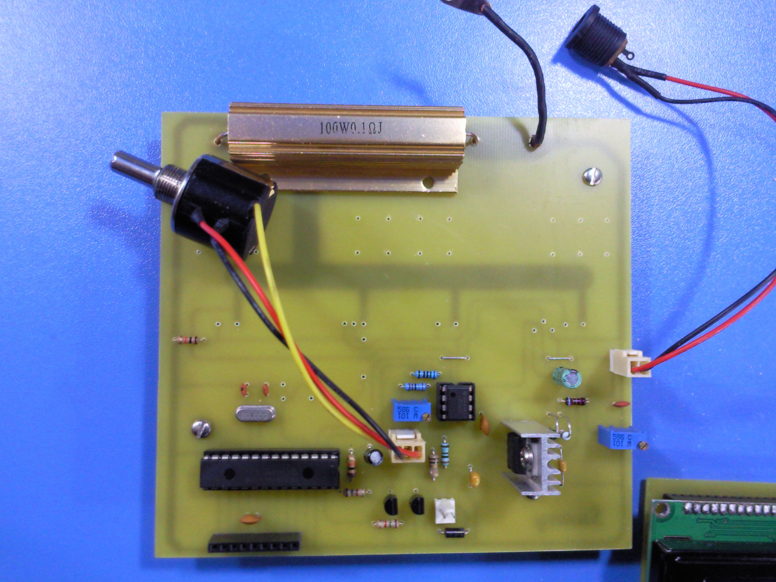
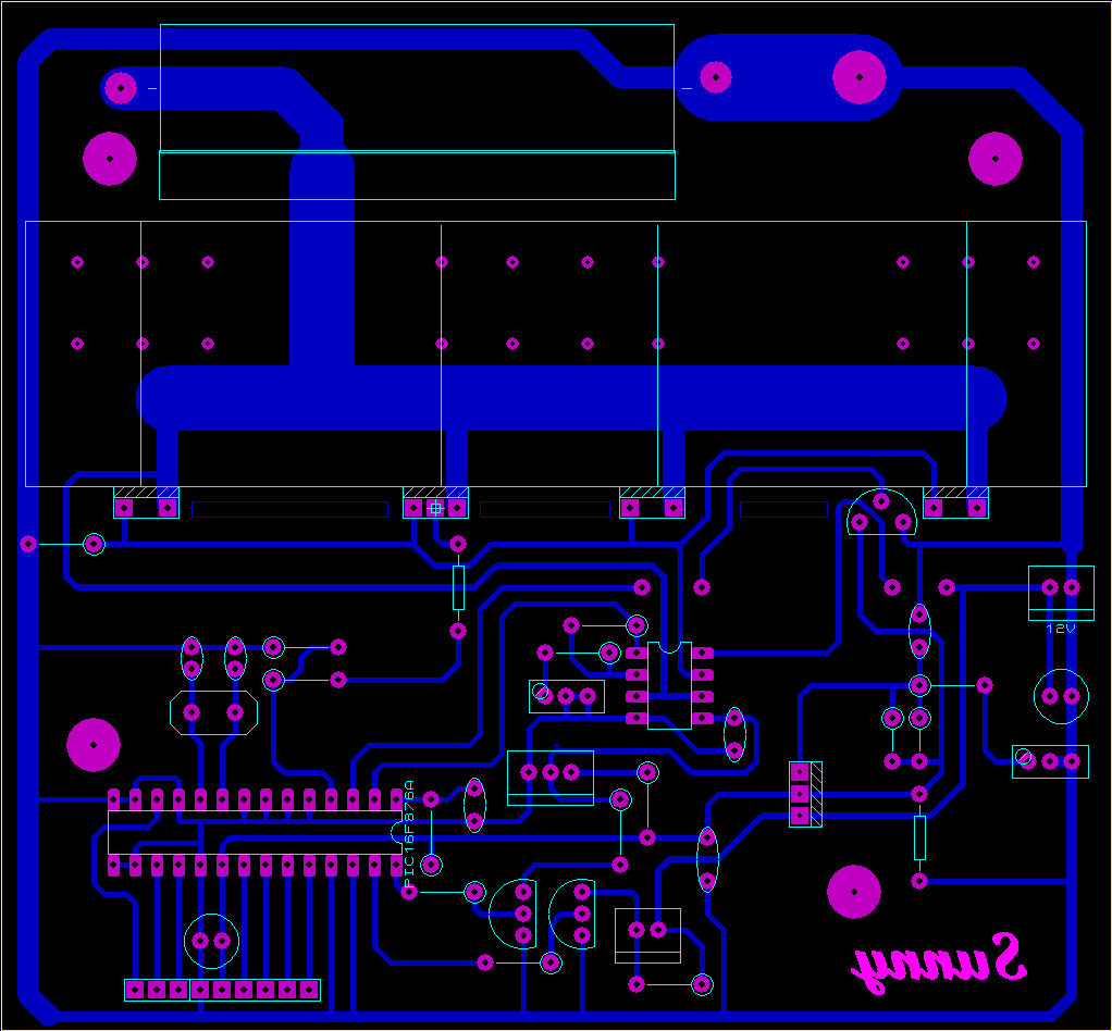
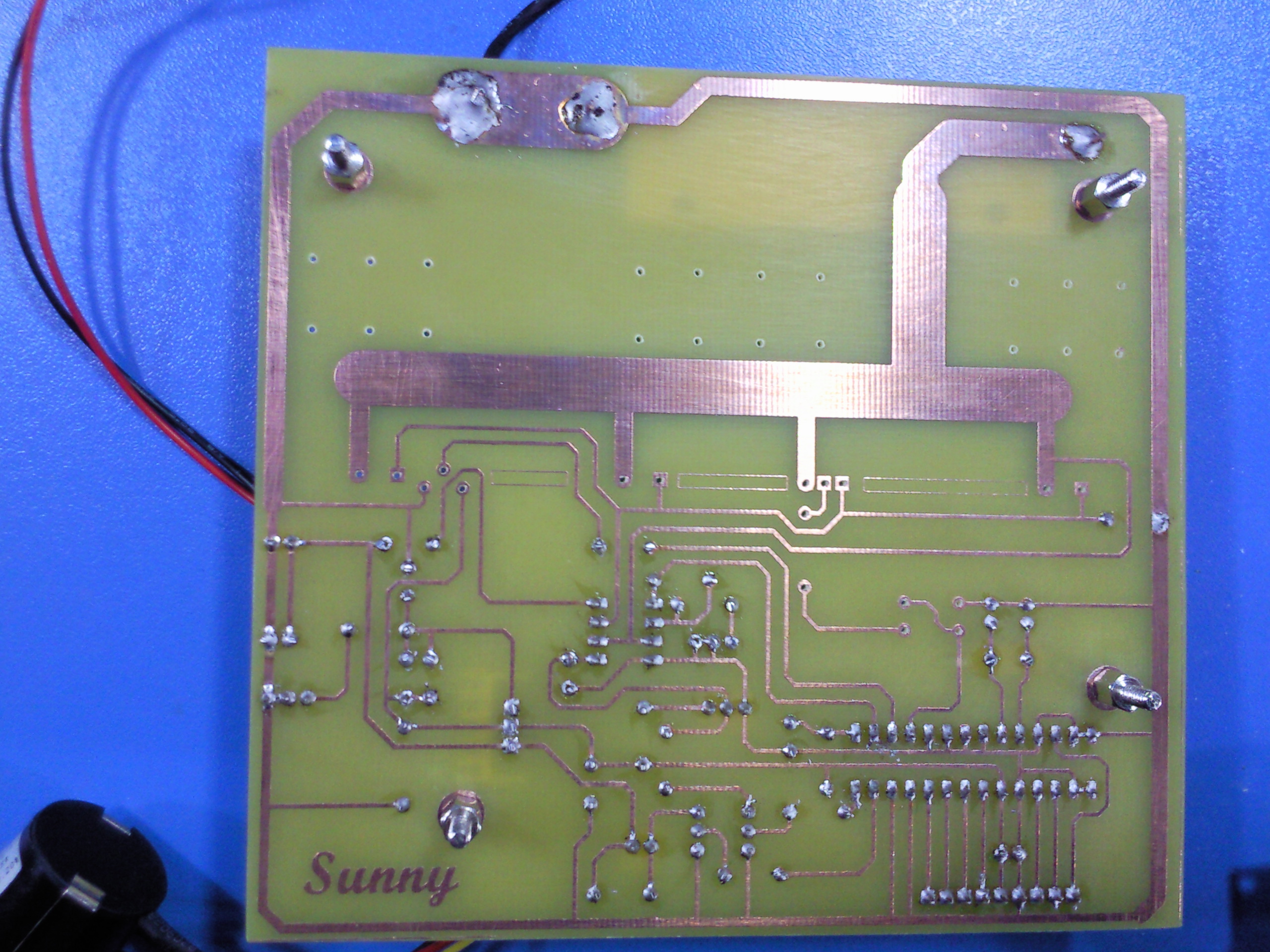
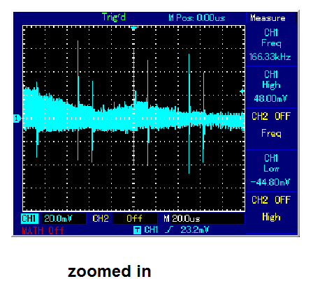
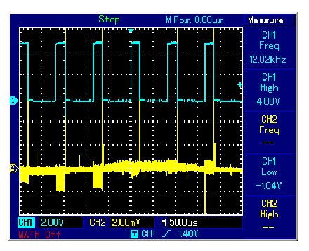
HI guys i am using PIC 16f876A and using its ADC by setting Vcc = 5.12 so that 5.12/1024 = 5mV exactly.I am using a 10 turns 500K pot and using a voltage buffer (with lm358). now the last digit is being changed like flikring i.e. 1024 and the digit is 4. when i checked at the scope by probing the middle pin of the pot there was noise of 7 to 9 mV....gotya. i have tried even a 100nF bypass capacitor but this noise is not going way. the frequency of this noise varies from 11 to 16 MHz.

My guess is that 500K POT is picking up noise!:???:

I have read this article https://ww1.microchip.com/downloads/en/DeviceDoc/adn007.pdf but didn't understand. First he says the poor selection of devices,ok i get it. i have to see the data sheet for there noise issue. 2nd he says conducted noise and 3rd he says EMI noise, didn't get it. and what is "ground plane" terminology.

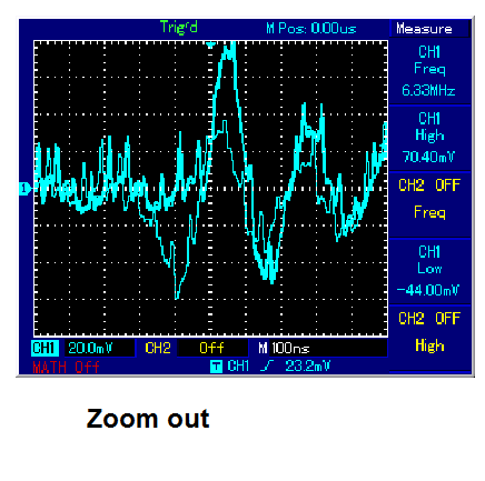
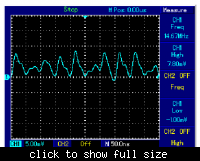
PIC of noise signal is added.


Do u have noise when dac input shorted ?
 

Its an ADC. I have noticed another thing that the PCB track from LM358 Ground to PIC ground is 4 inches away and is 20th of an inch in width. there is no noise between the two point and when i place the pic in the holder then there i see the noise.


Reduce input impedance, should not be greater than 10K.
 

In a setup as described, mV voltages at MHz frequency don't have to do with the real voltage at the chip. The measurement mainly tells that you managed to pick up some interferences with you oscilloscope probe. It can be of course expected, that similar interferences exist at the chip. But even without a bypass capacitor, the ADC sampling circuit has a maximum bandwidth of about 200 kHz, so the interference should be attenuated far below ADC resolution inside the chip.

It's pretty reasonable to keep the said suggestions about low impedance ADC sources anyway.
 
You can use some dedicated reference voltage source like MCP1541 which outputs 4.096V +/- 1%, 50 ppm/*C. Use 100nF ceramic + 1uF (or 10uF) tantalum across reference power supply and reference output. Use 100n+10u across each pair of PIC VCC pins. Use separate voltage straight from regulator for AVCC. Each supply point to mcu/ref voltage source should be passed through small choke as close as physically possible to power pins. That's basic stuff. You can also use separate ground planes for analog and digital voltages (this is optional if placement is done correctly) and separate power lines for analog and digital signals straight from regulator (that's mandatory).

Depending on your input signal type (dc, lf? what frequency?) build and LC or RC filter on ADC input to filter frequencies above 1/2 of sampling frequency.

Signal you have observed with oscilloscope is probably some general noise, but if your circuit is designed poorly it might be for example clocking frequency of PIC coupling into input signal.
 
Yep i doubt about the 500K POT too. bought 1K today so tell you after checking. Also i wana ask that LM358 has the max offset of 7mV. this can be an issue too? any suggestions? I also read somewhere that if some of your controller pins are not being used then set them to digital input and ground them. Anyways i am etching a new PCB now so tell u after that.

By the away whats with ur display pics ALTER:-D

---------- Post added at 20:37 ---------- Previous post was at 20:31 ----------

Ok so how you guys decide like what value should be placed for bypassing? i know that low value cap filters high frequencies and High value cap filters low noises but i don't know how to calculate exact value.

---------- Post added at 20:44 ---------- Previous post was at 20:37 ----------

PIC and ADC are in one chip package so i cant use separate regulators, rest LM358 is powered with 12V and same 12 is regulated to 5.12v for PIC..By choke you mean that ferrite ring and wires wound across it? but for that how may turns and flux density of core???? I understand your point that since it acts like inductor so any switching in PIC will not go back to regulator as inductor blocks instant current rise so it won't distribute to other components,right?
 

The low impedance should be on PIC adc pin. You can put 4.7K fixed resistor on the pin and ground. It will damp noise.
 
Last edited:

If the band with is 200khz then u may have some parasitic oscillation between pic leads.
Sorry like i know no homemade etch can be that perfect like ready make even the board material is important..
maybe u send the diagram and the etch-layout and we can see if using a a few 10pf capacitors on some lpic leads help.
have u done the circuit on breadboard first ?
 

Yep i doubt about the 500K POT too. bought 1K today so tell you after checking. Also i wana ask that LM358 has the max offset of 7mV. this can be an issue too? any suggestions? I also read somewhere that if some of your controller pins are not being used then set them to digital input and ground them. Anyways i am etching a new PCB now so tell u after that.

By the away whats with ur display pics ALTER:-D

---------- Post added at 20:37 ---------- Previous post was at 20:31 ----------

Ok so how you guys decide like what value should be placed for bypassing? i know that low value cap filters high frequencies and High value cap filters low noises but i don't know how to calculate exact value.

---------- Post added at 20:44 ---------- Previous post was at 20:37 ----------

PIC and ADC are in one chip package so i cant use separate regulators, rest LM358 is powered with 12V and same 12 is regulated to 5.12v for PIC..By choke you mean that ferrite ring and wires wound across it? but for that how may turns and flux density of core???? I understand your point that since it acts like inductor so any switching in PIC will not go back to regulator as inductor blocks instant current rise so it won't distribute to other components,right?

You shouldn't have any problem with impedance, since, after the 500k pot, you're using a buffer (voltage follower). Between the buffer output and the ADC input, place a 1k resistor and a 1nF-10nF capacitor from the ADC pin to ground.

Try this and let us know.

Hope this helps.
Tahmid.
 

There are several hardware and software prerequisites to achieve full resolution with on-chip ADCs of PIC and similar processors. The observed high frequency signal is just an indication of existing signal integrity problems but necessarily the cause of poor ADC results.
 

ok made a new PCB. Now situation is much worst. even though i have put 0.01uf ceramic cap near controller pin and its Gnd to controller Gnd. I have put 1uf Cap Solid tantlum at regulator output. 0.01 uF cap on the POT mid pin. and POT is now 1K. i have average noise of 16mV of MHZ frequency and when i zoom out, spikes of 63mV were detected on POT mid pin. Confirmed thing is that it all happens when i put the controller in socket and when i pull it out...noise gone just 1.6mV of noise left.

And i tried both 12V supply SMPS, and liner but same result. There was ringing effect detected with SMPS but it was then when i used 500K POT.

I hope you guys understand the layout while comparing to the original PCB.


Zoom in = zoom out
Zoom out = zoom in......sorry my mistake:wink:
 
Last edited:

! dont get it .
Your smps show 3000 turns versus 1 turn ???
1_1328540863.jpg
looks like some kind of current transformer
see this link is that what u doing ?
Voltmeter Ammeter
 
Last edited:

! dont get it .
Your smps show 3000 turns versus 1 turn ???
View attachment 68846
looks like some kind of current transformer

How can u say 3000 turns, where did that come from!!!!!!

There is no SMPS on board. Its an external power supply which connects to the power jack with red and black wires.
 

It says so read it right under the coil drawing n1 3000t n2 1t

1_1328540863  expanded.jpg
 

Confused didnt u send me this mail ?

"Dear dselec,

Sajjadkhan has just replied to a thread you have subscribed to entitled - 10 bit ADC noise in Circuit. - in the Analog Circuit Design forum of Forum for Electronics.

This thread is located at:


Here is the message that has just been posted:
***************
ok made a new PCB. Now situation is much worst. even though i have put 0.01uf ceramic cap near controller pin and its Gnd to controller Gnd. I have put 1uf Cap Solid tantlum at regulator output. 0.01 uF cap on the POT mid pin. and POT is now 1K. i have average noise of 16mV of MHZ frequency and when i zoom out, spikes of 63mV were detected on POT mid pin. Confirmed thing is that it all happens when i put the controller in socket and when i pull it out...noise gone just 1.6mV of noise left.

And i tried both 12V supply SMPS, and liner but same result. There was ringing effect detected with SMPS but it was then when i used 500K POT.

I hope you guys understand the layout while comparing to the original PCB.

Image: https://obrazki.elektroda.pl/21_1328699672_thumb.jpg (https://obrazki.elektroda.pl/21_1328699672.jpg) Image: https://obrazki.elektroda.pl/82_1328699673_thumb.jpg (https://obrazki.elektroda.pl/82_1328699673.jpg) Image: https://obrazki.elektroda.pl/25_1328699673_thumb.jpg (https://obrazki.elektroda.pl/25_1328699673.jpg) Image: https://obrazki.elektroda.pl/67_1328699673_thumb.png (https://obrazki.elektroda.pl/67_1328699673.png) Image: https://obrazki.elektroda.pl/61_1328699673_thumb.jpg (https://obrazki.elektroda.pl/61_1328699673.jpg)
Image: https://obrazki.elektroda.pl/2_1328699736_thumb.png (https://obrazki.elektroda.pl/2_1328699736.png) Image: https://obrazki.elektroda.pl/46_1328699736_thumb.png (https://obrazki.elektroda.pl/46_1328699736.png)
***************


There may also be other replies, but you will not receive any more notifications until you visit the forum again.

All the best,
Forum for Electronics "
 

i didn't send it, EDA board sent it and the link bring back u here. Still this mail has nothing to do with 3000 vs 1 turn transformer.

---------- Post added at 18:05 ---------- Previous post was at 18:04 ----------

U just replied to wrong post.
 

ok now i am building from the scrap. On bread board there is only PIC, 12MHZ OSC, 7805 regulator. All pins of ADC are grounded except AN0 which is grounded through 1.5K resistor. PWM is activated on RC1 pin. Noise is of max 1.7mV but i am seeing spikes on AN0. These spikes occur when pwm channel transition goes from high to low as u can see in the fig,.

---------- Post added at 11:10 ---------- Previous post was at 11:03 ----------

 
Last edited:

- some crosstalk can't be avoided in mixed-signal chips
- with your limited equipment, you'll face difficulties to determine for sure if the signal is actually present at the analog pin or just a measurement artefact. Let's assume for the time being that it's real.
- a low interference mixed signal design requires other techniques than a single layer PCB with cm long thin ground traces. You have to accept some level of "noise" with your kind of boards.

As a cross-check, it would be interesting to determine the ADC value variation with PWM off. There may be an addtional problem of unsuitable ADC operation parameters (clock, acquisition time). If the problem turns out to be mostly caused by external interferences, averaging and digital filtering can be still a way.
 
Status
Not open for further replies.

Similar threads

Part and Inventory Search

Welcome to EDABoard.com

Sponsor

Back
Top