Getting a solid grasp of static timing analysis in digital circuits can be a very big challenge. It usually takes quite a bit of experience. In my view it’s not covered very well in school, and because of that it’s more difficult for new engineers.
I’ll attempt to cover this topic in depth here. We’ll start with most simplest case, which is a basic flip-flop timing path.
In general digital circuits have two types of elements,
1) combinational elements which include logic gates like, NAND gate, NOR gate, COMPLEX gate etc..
2) storage elements or memory elements, which are either flip-flops or latches. Flip-flops, which will be abbreviated as flops, are edge triggered memory elements, while latches are level sensitive memory elements.
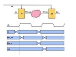
Following is a simple structure where output of a flop goes through some stages of combinational logic, represented by pink bubble and is eventually samples by receiving flop. Receiving flop, which samples the FF2_in data, poses timing requirements on the input data signal.
The logic between FF1_out to FF2_in should be such that signal transitions could propagate through this logic fast enough to be captured by the receiving flop. For a flop to correctly capture input data, the input data to flop has to arrive and become stable for some period of time before the capture clock edge at the flop.
This requirement is called the setup time of the flop. Usually you’ll run into setup time issues when there is too much logic in between two flop or the combinational delay is too small. Hence this is sometimes called max delay or slow delay timing issue and the constraints is called max delay constraint.
In figure there is max delay constraint on FF2_in input at receiving flop. Now you can realize that max delay or slow delay constraint is frequency dependent. If you are failing setup to a flop and if you slow down the clock frequency, your clock cycle time increases, hence you’ve larger time for your slow signal transitions to propagate through and you’ll now meet setup requirements.
Typically your digital circuit is run at certain frequency which sets your max delay constraints. Amount of time the signal falls short to meet the setup time is called setup or max, slack or margin. There is flip side to max delay constraint which is min or fast delay constraint.
It more interesting and difficult to understand hence will cover in next post. Following figure shows the data propagation from input to the output of the flop and through combinational delay to the input of next flop.
Be aware that data FF1_out potentially changes( if ‘in’ chnages ) on the active/capture edge of the flop, in following case we’ve assumed flops to be rising edge triggered.

I’ll attempt to cover this topic in depth here. We’ll start with most simplest case, which is a basic flip-flop timing path.
In general digital circuits have two types of elements,
1) combinational elements which include logic gates like, NAND gate, NOR gate, COMPLEX gate etc..
2) storage elements or memory elements, which are either flip-flops or latches. Flip-flops, which will be abbreviated as flops, are edge triggered memory elements, while latches are level sensitive memory elements.
Following is a simple structure where output of a flop goes through some stages of combinational logic, represented by pink bubble and is eventually samples by receiving flop. Receiving flop, which samples the FF2_in data, poses timing requirements on the input data signal.
The logic between FF1_out to FF2_in should be such that signal transitions could propagate through this logic fast enough to be captured by the receiving flop. For a flop to correctly capture input data, the input data to flop has to arrive and become stable for some period of time before the capture clock edge at the flop.
This requirement is called the setup time of the flop. Usually you’ll run into setup time issues when there is too much logic in between two flop or the combinational delay is too small. Hence this is sometimes called max delay or slow delay timing issue and the constraints is called max delay constraint.
In figure there is max delay constraint on FF2_in input at receiving flop. Now you can realize that max delay or slow delay constraint is frequency dependent. If you are failing setup to a flop and if you slow down the clock frequency, your clock cycle time increases, hence you’ve larger time for your slow signal transitions to propagate through and you’ll now meet setup requirements.
Typically your digital circuit is run at certain frequency which sets your max delay constraints. Amount of time the signal falls short to meet the setup time is called setup or max, slack or margin. There is flip side to max delay constraint which is min or fast delay constraint.
It more interesting and difficult to understand hence will cover in next post. Following figure shows the data propagation from input to the output of the flop and through combinational delay to the input of next flop.
Be aware that data FF1_out potentially changes( if ‘in’ chnages ) on the active/capture edge of the flop, in following case we’ve assumed flops to be rising edge triggered.