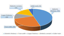
Trace width, the impedance trace width is inversely with the impedance value, the thinner the trace is, the larger the impedance value.
Space, not only the space between the impedance traces will affect the impedance value, but the ground copper around the impedance traces. Impedance traces spacing is proportional to the impedance value, the smaller the space, the smaller the impedance value.
Copper thickness, it is inversely with the impedance value, the thicker the copper, the smaller the impedance value.
Dielectric thickness, it is the thickness between the shielding layer and the impedance traces. Dielectric thickness is proportional to the impedance value, the thicker the dielectric, the larger the impedance value.
Dielectric constant, it is inversely with the impedance value, the larger the dielectric constant, the smaller the impedance value.
The thickness of the solder resist also will affect the impedance value, but it is usually ignored by the designer.