Continue to Site

Welcome to EDAboard.com

Welcome to our site! EDAboard.com is an international Electronics Discussion Forum focused on EDA software, circuits, schematics, books, theory, papers, asic, pld, 8051, DSP, Network, RF, Analog Design, PCB, Service Manuals... and a whole lot more! To participate you need to register. Registration is free. Click here to register now.

SPI clock optimization in stm32h745

dbp

Newbie level 4
Joined
May 16, 2024
Messages
6
Helped
0
Reputation
0
Reaction score
0
Trophy points
1
Activity points
57
Hello team,
I have to interface the ADS7046 12-Bit, 3-MSPS, Single-Ended Input, Small-Size, Low-Power SAR ADC with STM32H745iik6 controller. SPI compatible ADC 12 bit resolution and MSPS.
So as my code ADC read properly but sampling rate does not get as my desired.
My challenges is that
1) how to get 3msps means CS falling edge to falling edge (Tcycle=333nS) required. as datasheet mention timing diagram below.
1715849771314.png


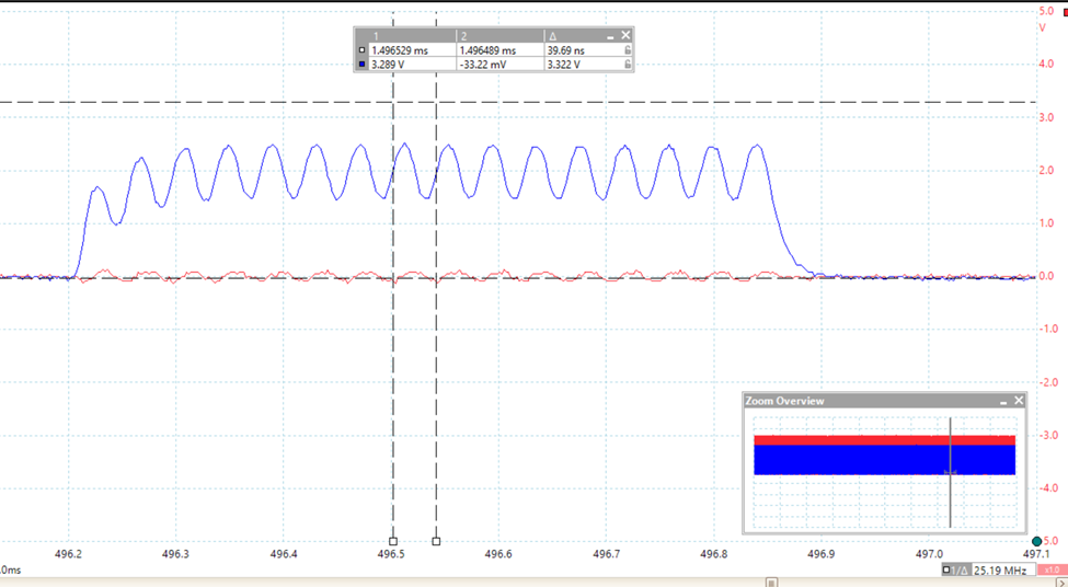
But I got approx. 5uS. SPI read with polling method and CS simple gpio. below attach some snap of scope and code.... Red= CS, Blue= Sclk 16pulse
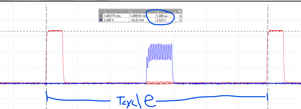
1715850625238.png

1715851402725.png


C:
    for (int m = 0; m < 500; m++) {
                HAL_GPIO_WritePin(GPIOG, SPI3_CS3_Pin,GPIO_PIN_RESET);         // SPI3 TL1_VMEAS
       //     HAL_SPI_Receive_IT(&hspi3, (uint8_t*)&ADC_Value3,1);
          HAL_SPI_Receive(&hspi3, (uint8_t*)&ADC_Value3, 1, HAL_MAX_DELAY);
          buff3[m] =ADC_Value3;
 //       OUTPUT_VOLTAGE3=((3.3/4095)*ADC_Value3/4);
                HAL_GPIO_WritePin(GPIOG, SPI3_CS3_Pin,GPIO_PIN_SET);         // SPI3 TL1_VMEAS

     }
                    // Transmit USB packets after i reaches 500
                    for (int j = 0; j < 500; j++) {
                        sprintf(buffer3, "%d\n\r", buff3[j]);
                        CDC_Transmit_FS((uint8_t *)buffer3, strlen(buffer3));
                     //   delay_us(10);
                        memset(buffer3,'\0',sizeof(buffer3));
                    }

                    m = 0;
                    memset(buff3,'\0',sizeof(buff3));


in above code i read 500 sample and store in buffer then print using usb.

So i applied input square awve waveform but as my observation upto 40Mhz square read good then aliasing occure....
i just want to fast spi read...

2) how to minimize sclk pulse regenrate time. means spi generate 16 pulse then it take 5uS delay then again generate. there is no issue in gpio. just want to minimize off time of sclk . how can i minimize...
without CS also taking same time for sclk.
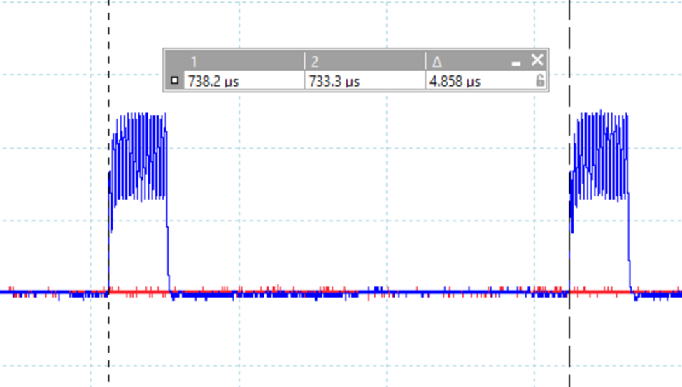
1715851327157.png


i set my controller clock frequency as below.
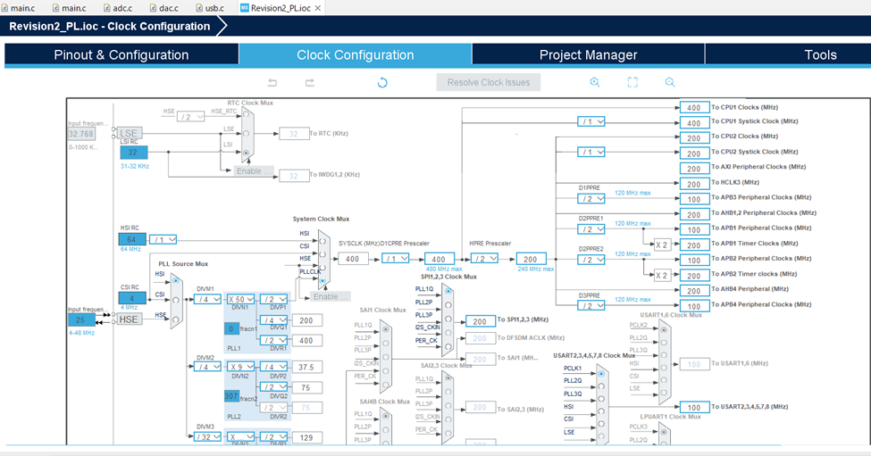
1715851358551.png
 
Hi,

I´m not familiar with your STM .. thus I don´t know all features.

With other microcontrollers I did it this way:

* Set up a buffer for 500x 2 bytes to store the SPI_receive results
* set up the SPI for the SS to be controlled "manually" (i.e. not by software), and all other parameters for proper operation.
* set up an PWM periferal to generate the SS signal. 3MHz with a suitable duty cycle

* On every falling edge of SS start 16 bit SPI transfer. Store the results in buffer, mybe via DMA.

***
Then the PWM controls the sampling rate. It will be perfectly timed, accurate frequency, low jitter.
And the SPI periferal is just responsible for the proper data transfer. SPI clock delay (from SS falling) and speed is uncritical ... as long as it it fast enough to transfer all bits according ADS datasheet.

***
As said: The STM may provide a better solution like this. Reading the datsheet is essential.

****
Added:
Btw: why an externmal 3MHz 12 bit ADC while the STM includes an 3.6MHz 12 bit ADC?

Klaus
 
Hello!

With STM32, you have better ways to automaticlly import data into buffers. Never did it with SPI, but with the audio
input. You configure one buffer, and you can configure an interrupt at half of the buffer.
Once the interrupt is called, you don't have to do anything other than processing your data, and when finsihed
you just have to wait for the next interrupt. And ST "knows" where to write, it's automagically cyclic.

Again, I have never done it with SPI, but it's worth looking at the documentation.

Dora.
 
Thanks for replying @KlausST and @doraemon.

I use buffer for storing purpose and there is an no impact on SPI timing...
1) I want how can i read spi very fast speed.
using only below command in continue while(1) loop it taking same delay between regenerate. means spi taking long time to process.

HAL_SPI_Receive(&hspi3, (uint8_t*)&ADC_Value3, 1, 0);
1715862781423.png


any possibility to minimize this time is HAL code.

2) This time i control using increasing process clock speed. means before i use my controller clock 180Mhz that time approx.20uS there. but now i increase controller clock 400Mhz max then it taking approx.5uS.

STM32h745iik6 controller as 480Mhz Max clock frequency but for highest not working.

3) Suppose I read 3 ADC in parallel using interleaving method as refer below.
can you guide me?
 
Hi,

means spi taking long time to process.
I already answered: Use DMA. This minimizes processing power. No need to wait for data being transferred.

3) Suppose I read 3 ADC in parallel using interleaving method as refer below.
What? Now you have three in parallel? How? You never mentioned this before. No schematic either.
What other imortant informations do you hide?

For me speaking: I will continue the discussion only if we get all informatins at once. I don´t want to spend time to answer questions ... which turns out to be useless after you come with new informations.

Klaus
 
How do you manage to get such a bad SCLK waveform? Unsuitable oscilloscope probe, wrong oscilloscope settings, large load capacitance?
 
Hi,


I already answered: Use DMA. This minimizes processing power. No need to wait for data being transferred.


What? Now you have three in parallel? How? You never mentioned this before. No schematic either.
What other imortant informations do you hide?

For me speaking: I will continue the discussion only if we get all informatins at once. I don´t want to spend time to answer questions ... which turns out to be useless after you come with new informations.

Klaus
I also trying to read with dma but same processing time there also. means it take 9uS. can you provide one example code with DMA . how to configure, buffere size, which channer need to select for spi1.


2) as talk three ADC is next plan if sampling rate not achieve using one adc. in below schematic i applied input to opa836 as a buffer and then 3adc in parrallel... as sharing datasheet above msgs. 3) ignore my all clues. give me just straightforward way to read spi fast. and how can i use DMA. or any code plz send.
1715919694307.png
 
Hi,
I also trying to read with dma but same processing time there also. means it take 9uS. can you provide one example code with DMA . how to configure, buffere size, which channer need to select for spi1.
If set up correctly the DMA read takes zero processing power for all 500 x 2 bytes.
You never do a "WHILE(spi_does_something)"
Do you understand the basic concept of DMA?

I don´t have example codes, but there is plenty in the internet. ... with explanations, even videos.

For sure you are free to post your code. There will be people to help you to rectify it.

Klaus
--- Updated ---

No. it bcoz of high sclk frequency...
I don´t think so.
I´m more then 95% sure it´s a measurement problem.

Klaus
 
No. it bcoz of high sclk frequency...
OK - so what is the SCLK frequency?
The ADC has a max clock frequency of 60MHz, and the SPI module on the MCU can do that easily (see Table 106), and also the IO ports can transition that fast (table 160, 161).
What is the bandwidth of your scope?

As for the DMA examples, are you using the STM32CUBE IDE? It will generate most of the code for you.
Susan
Yes susan, now SCLK frequency is 25Mhz. and yes i also working with 50Mhz SCLK frequency but that some data lapse so now i used 25mhz now. and picoscope specification is 8bits at 1GSPS and bandwidth 50Mhz.

2) yes i'm using stm32cubeide 1.15.0. can you please suggest for DMA activated process?
1716180992042.png

1716181036952.png
1716181119233.png
1716181152720.png
 
OK - so what is the SCLK frequency?
The ADC has a max clock frequency of 60MHz, and the SPI module on the MCU can do that easily (see Table 106), and also the IO ports can transition that fast (table 160, 161).
What is the bandwidth of your scope?

As for the DMA examples, are you using the STM32CUBE IDE? It will generate most of the code for you.
Susan
I setup spi DMA as above and code as below it read for constant DC input. but i want to read waveforms so it read lower frequency waveform upto 5khz but not read above high frequency waveform means sampling rate not as expected.
C:
/* USER CODE BEGIN Header */
/**
  ******************************************************************************
  * @file           : main.c
  * @brief          : Main program body
  ******************************************************************************
  * @attention
  *
  * Copyright (c) 2024 STMicroelectronics.
  * All rights reserved.
  *
  * This software is licensed under terms that can be found in the LICENSE file
  * in the root directory of this software component.
  * If no LICENSE file comes with this software, it is provided AS-IS.
  *
  ******************************************************************************
  */
/* USER CODE END Header */
/* Includes ------------------------------------------------------------------*/
#include "main.h"
#include "usb_device.h"

/* Private includes ----------------------------------------------------------*/
/* USER CODE BEGIN Includes */
#include <stdio.h>
#include "usbd_cdc_if.h"
#include <string.h>
/* USER CODE END Includes */

/* Private typedef -----------------------------------------------------------*/
/* USER CODE BEGIN PTD */

/* USER CODE END PTD */

/* Private define ------------------------------------------------------------*/
/* USER CODE BEGIN PD */

#ifndef HSEM_ID_0
#define HSEM_ID_0 (0U) /* HW semaphore 0*/
#endif

/* USER CODE END PD */

/* Private macro -------------------------------------------------------------*/
/* USER CODE BEGIN PM */

/* USER CODE END PM */

/* Private variables ---------------------------------------------------------*/

SPI_HandleTypeDef hspi3;
DMA_HandleTypeDef hdma_spi3_rx;

TIM_HandleTypeDef htim2;

/* USER CODE BEGIN PV */

/* USER CODE END PV */

/* Private function prototypes -----------------------------------------------*/
void SystemClock_Config(void);
void PeriphCommonClock_Config(void);
static void MPU_Config(void);
static void MX_GPIO_Init(void);
static void MX_DMA_Init(void);
static void MX_SPI3_Init(void);
static void MX_TIM2_Init(void);
/* USER CODE BEGIN PFP */
uint16_t m=0;
uint16_t buff[500];
uint16_t buff1[500];
uint16_t i = 0;
uint16_t Rx_data[1] = {0};
uint16_t Rxflag = 0;
/* USER CODE END PFP */

/* Private user code ---------------------------------------------------------*/
/* USER CODE BEGIN 0 */

/* USER CODE END 0 */

/**
  * @brief  The application entry point.
  * @retval int
  */
int main(void)
{

  /* USER CODE BEGIN 1 */

  /* USER CODE END 1 */
/* USER CODE BEGIN Boot_Mode_Sequence_0 */
  int32_t timeout;
/* USER CODE END Boot_Mode_Sequence_0 */

  /* MPU Configuration--------------------------------------------------------*/
  MPU_Config();

/* USER CODE BEGIN Boot_Mode_Sequence_1 */
  /* Wait until CPU2 boots and enters in stop mode or timeout*/
  timeout = 0xFFFF;
  while((__HAL_RCC_GET_FLAG(RCC_FLAG_D2CKRDY) != RESET) && (timeout-- > 0));
  if ( timeout < 0 )
  {
  Error_Handler();
  }
/* USER CODE END Boot_Mode_Sequence_1 */
  /* MCU Configuration--------------------------------------------------------*/

  /* Reset of all peripherals, Initializes the Flash interface and the Systick. */
  HAL_Init();

  /* USER CODE BEGIN Init */

  /* USER CODE END Init */

  /* Configure the system clock */
  SystemClock_Config();

/* Configure the peripherals common clocks */
  PeriphCommonClock_Config();
/* USER CODE BEGIN Boot_Mode_Sequence_2 */
/* When system initialization is finished, Cortex-M7 will release Cortex-M4 by means of
HSEM notification */
/*HW semaphore Clock enable*/
__HAL_RCC_HSEM_CLK_ENABLE();
/*Take HSEM */
HAL_HSEM_FastTake(HSEM_ID_0);
/*Release HSEM in order to notify the CPU2(CM4)*/
HAL_HSEM_Release(HSEM_ID_0,0);
/* wait until CPU2 wakes up from stop mode */
timeout = 0xFFFF;
while((__HAL_RCC_GET_FLAG(RCC_FLAG_D2CKRDY) == RESET) && (timeout-- > 0));
if ( timeout < 0 )
{
Error_Handler();
}
/* USER CODE END Boot_Mode_Sequence_2 */

  /* USER CODE BEGIN SysInit */

  /* USER CODE END SysInit */

  /* Initialize all configured peripherals */
  MX_GPIO_Init();
  MX_DMA_Init();
  MX_USB_DEVICE_Init();
  MX_SPI3_Init();
  MX_TIM2_Init();
  /* USER CODE BEGIN 2 */
  HAL_GPIO_WritePin(GPIOD, GPIO_PIN_13, GPIO_PIN_RESET);
  HAL_GPIO_WritePin(GPIOG, GPIO_PIN_1, GPIO_PIN_SET);
    memset(buff,'\0',sizeof(buff));
    memset(buff1,'\0',sizeof(buff1));
//    uint16_t ADC_Value3=0;
  /* USER CODE END 2 */
    HAL_TIM_Base_Start(&htim2);
    HAL_GPIO_WritePin(GPIOG, GPIO_PIN_1, GPIO_PIN_RESET);
    HAL_SPI_Receive_DMA(&hspi3,(uint8_t *)Rx_data, 1);
    HAL_GPIO_WritePin(GPIOG, GPIO_PIN_1, GPIO_PIN_SET);
  /* Infinite loop */
  /* USER CODE BEGIN WHILE */
while (1)
{

    if (Rxflag == 1)
    {
        Rxflag = 0;
  //      for (int m = 0; m < 500; m++) {
           sprintf(buff1, "%d\n\r", Rx_data[0]);
            CDC_Transmit_FS((uint8_t *)buff1, strlen(buff1));
            memset(Rx_data,0,sizeof(Rx_data));
        HAL_GPIO_WritePin(GPIOG, GPIO_PIN_1, GPIO_PIN_RESET);
        HAL_SPI_Receive_DMA(&hspi3,(uint8_t *)Rx_data, 1);
//        buff[m] = Rx_data[0];
        HAL_GPIO_WritePin(GPIOG, GPIO_PIN_1, GPIO_PIN_SET);
      //  }

//         for (int j = 0; j < 500; j++) {
//                sprintf(buff1, "%d\n\r", buff[j]);
//                CDC_Transmit_FS((uint8_t *)buff1, strlen(buff1));
//            }
//             m = 0;
//            memset(buff,'\0',sizeof(buff));
//            memset(buff1,'\0',sizeof(buff1));
    }
    /* USER CODE END WHILE */

    /* USER CODE BEGIN 3 */
  }
  /* USER CODE END 3 */
}


void HAL_SPI_RxCpltCallback(SPI_HandleTypeDef *hspi)
{
     if(hspi3.Instance == SPI3)
     {
         Rxflag = 1;
     }
}
/**
  * @brief System Clock Configuration
  * @retval None
  */
void SystemClock_Config(void)
{
  RCC_OscInitTypeDef RCC_OscInitStruct = {0};
  RCC_ClkInitTypeDef RCC_ClkInitStruct = {0};

  /** Supply configuration update enable
  */
  HAL_PWREx_ConfigSupply(PWR_EXTERNAL_SOURCE_SUPPLY);

  /** Configure the main internal regulator output voltage
  */
  __HAL_PWR_VOLTAGESCALING_CONFIG(PWR_REGULATOR_VOLTAGE_SCALE0);

  while(!__HAL_PWR_GET_FLAG(PWR_FLAG_VOSRDY)) {}

  /** Initializes the RCC Oscillators according to the specified parameters
  * in the RCC_OscInitTypeDef structure.
  */
  RCC_OscInitStruct.OscillatorType = RCC_OSCILLATORTYPE_HSI48|RCC_OSCILLATORTYPE_HSE;
  RCC_OscInitStruct.HSEState = RCC_HSE_ON;
  RCC_OscInitStruct.HSI48State = RCC_HSI48_ON;
  RCC_OscInitStruct.PLL.PLLState = RCC_PLL_ON;
  RCC_OscInitStruct.PLL.PLLSource = RCC_PLLSOURCE_HSE;
  RCC_OscInitStruct.PLL.PLLM = 2;
  RCC_OscInitStruct.PLL.PLLN = 64;
  RCC_OscInitStruct.PLL.PLLP = 2;
  RCC_OscInitStruct.PLL.PLLQ = 4;
  RCC_OscInitStruct.PLL.PLLR = 2;
  RCC_OscInitStruct.PLL.PLLRGE = RCC_PLL1VCIRANGE_3;
  RCC_OscInitStruct.PLL.PLLVCOSEL = RCC_PLL1VCOWIDE;
  RCC_OscInitStruct.PLL.PLLFRACN = 0;
  if (HAL_RCC_OscConfig(&RCC_OscInitStruct) != HAL_OK)
  {
    Error_Handler();
  }

  /** Initializes the CPU, AHB and APB buses clocks
  */
  RCC_ClkInitStruct.ClockType = RCC_CLOCKTYPE_HCLK|RCC_CLOCKTYPE_SYSCLK
                              |RCC_CLOCKTYPE_PCLK1|RCC_CLOCKTYPE_PCLK2
                              |RCC_CLOCKTYPE_D3PCLK1|RCC_CLOCKTYPE_D1PCLK1;
  RCC_ClkInitStruct.SYSCLKSource = RCC_SYSCLKSOURCE_PLLCLK;
  RCC_ClkInitStruct.SYSCLKDivider = RCC_SYSCLK_DIV1;
  RCC_ClkInitStruct.AHBCLKDivider = RCC_HCLK_DIV2;
  RCC_ClkInitStruct.APB3CLKDivider = RCC_APB3_DIV2;
  RCC_ClkInitStruct.APB1CLKDivider = RCC_APB1_DIV2;
  RCC_ClkInitStruct.APB2CLKDivider = RCC_APB2_DIV2;
  RCC_ClkInitStruct.APB4CLKDivider = RCC_APB4_DIV2;

  if (HAL_RCC_ClockConfig(&RCC_ClkInitStruct, FLASH_LATENCY_2) != HAL_OK)
  {
    Error_Handler();
  }
}

/**
  * @brief Peripherals Common Clock Configuration
  * @retval None
  */
void PeriphCommonClock_Config(void)
{
  RCC_PeriphCLKInitTypeDef PeriphClkInitStruct = {0};

  /** Initializes the peripherals clock
  */
  PeriphClkInitStruct.PeriphClockSelection = RCC_PERIPHCLK_TIM;
  PeriphClkInitStruct.TIMPresSelection = RCC_TIMPRES_ACTIVATED;

  if (HAL_RCCEx_PeriphCLKConfig(&PeriphClkInitStruct) != HAL_OK)
  {
    Error_Handler();
  }
}

/**
  * @brief SPI3 Initialization Function
  * @param None
  * @retval None
  */
static void MX_SPI3_Init(void)
{

  /* USER CODE BEGIN SPI3_Init 0 */

  /* USER CODE END SPI3_Init 0 */

  /* USER CODE BEGIN SPI3_Init 1 */

  /* USER CODE END SPI3_Init 1 */
  /* SPI3 parameter configuration*/
  hspi3.Instance = SPI3;
  hspi3.Init.Mode = SPI_MODE_MASTER;
  hspi3.Init.Direction = SPI_DIRECTION_2LINES_RXONLY;
  hspi3.Init.DataSize = SPI_DATASIZE_16BIT;
  hspi3.Init.CLKPolarity = SPI_POLARITY_LOW;
  hspi3.Init.CLKPhase = SPI_PHASE_1EDGE;
  hspi3.Init.NSS = SPI_NSS_SOFT;
  hspi3.Init.BaudRatePrescaler = SPI_BAUDRATEPRESCALER_4;
  hspi3.Init.FirstBit = SPI_FIRSTBIT_MSB;
  hspi3.Init.TIMode = SPI_TIMODE_DISABLE;
  hspi3.Init.CRCCalculation = SPI_CRCCALCULATION_DISABLE;
  hspi3.Init.CRCPolynomial = 0x0;
  hspi3.Init.NSSPMode = SPI_NSS_PULSE_ENABLE;
  hspi3.Init.NSSPolarity = SPI_NSS_POLARITY_LOW;
  hspi3.Init.FifoThreshold = SPI_FIFO_THRESHOLD_01DATA;
  hspi3.Init.TxCRCInitializationPattern = SPI_CRC_INITIALIZATION_ALL_ZERO_PATTERN;
  hspi3.Init.RxCRCInitializationPattern = SPI_CRC_INITIALIZATION_ALL_ZERO_PATTERN;
  hspi3.Init.MasterSSIdleness = SPI_MASTER_SS_IDLENESS_00CYCLE;
  hspi3.Init.MasterInterDataIdleness = SPI_MASTER_INTERDATA_IDLENESS_00CYCLE;
  hspi3.Init.MasterReceiverAutoSusp = SPI_MASTER_RX_AUTOSUSP_DISABLE;
  hspi3.Init.MasterKeepIOState = SPI_MASTER_KEEP_IO_STATE_DISABLE;
  hspi3.Init.IOSwap = SPI_IO_SWAP_DISABLE;
  if (HAL_SPI_Init(&hspi3) != HAL_OK)
  {
    Error_Handler();
  }
  /* USER CODE BEGIN SPI3_Init 2 */

  /* USER CODE END SPI3_Init 2 */

}

/**
  * @brief TIM2 Initialization Function
  * @param None
  * @retval None
  */
static void MX_TIM2_Init(void)
{

  /* USER CODE BEGIN TIM2_Init 0 */

  /* USER CODE END TIM2_Init 0 */

  TIM_ClockConfigTypeDef sClockSourceConfig = {0};
  TIM_MasterConfigTypeDef sMasterConfig = {0};

  /* USER CODE BEGIN TIM2_Init 1 */

  /* USER CODE END TIM2_Init 1 */
  htim2.Instance = TIM2;
  htim2.Init.Prescaler = 0;
  htim2.Init.CounterMode = TIM_COUNTERMODE_UP;
  htim2.Init.Period = 4294967295;
  htim2.Init.ClockDivision = TIM_CLOCKDIVISION_DIV1;
  htim2.Init.AutoReloadPreload = TIM_AUTORELOAD_PRELOAD_ENABLE;
  if (HAL_TIM_Base_Init(&htim2) != HAL_OK)
  {
    Error_Handler();
  }
  sClockSourceConfig.ClockSource = TIM_CLOCKSOURCE_INTERNAL;
  if (HAL_TIM_ConfigClockSource(&htim2, &sClockSourceConfig) != HAL_OK)
  {
    Error_Handler();
  }
  sMasterConfig.MasterOutputTrigger = TIM_TRGO_RESET;
  sMasterConfig.MasterSlaveMode = TIM_MASTERSLAVEMODE_DISABLE;
  if (HAL_TIMEx_MasterConfigSynchronization(&htim2, &sMasterConfig) != HAL_OK)
  {
    Error_Handler();
  }
  /* USER CODE BEGIN TIM2_Init 2 */

  /* USER CODE END TIM2_Init 2 */

}

/**
  * Enable DMA controller clock
  */
static void MX_DMA_Init(void)
{

  /* DMA controller clock enable */
  __HAL_RCC_DMA1_CLK_ENABLE();

  /* DMA interrupt init */
  /* DMA1_Stream0_IRQn interrupt configuration */
  HAL_NVIC_SetPriority(DMA1_Stream0_IRQn, 0, 0);
  HAL_NVIC_EnableIRQ(DMA1_Stream0_IRQn);

}

/**
  * @brief GPIO Initialization Function
  * @param None
  * @retval None
  */
static void MX_GPIO_Init(void)
{
  GPIO_InitTypeDef GPIO_InitStruct = {0};
/* USER CODE BEGIN MX_GPIO_Init_1 */
/* USER CODE END MX_GPIO_Init_1 */

  /* GPIO Ports Clock Enable */
  __HAL_RCC_GPIOA_CLK_ENABLE();
  __HAL_RCC_GPIOC_CLK_ENABLE();
  __HAL_RCC_GPIOD_CLK_ENABLE();
  __HAL_RCC_GPIOG_CLK_ENABLE();

  /*Configure GPIO pin Output Level */
  HAL_GPIO_WritePin(GPIOD, GPIO_PIN_13, GPIO_PIN_RESET);

  /*Configure GPIO pin Output Level */
  HAL_GPIO_WritePin(GPIOG, GPIO_PIN_1, GPIO_PIN_RESET);

  /*Configure GPIO pin : PD13 */
  GPIO_InitStruct.Pin = GPIO_PIN_13;
  GPIO_InitStruct.Mode = GPIO_MODE_OUTPUT_PP;
  GPIO_InitStruct.Pull = GPIO_NOPULL;
  GPIO_InitStruct.Speed = GPIO_SPEED_FREQ_VERY_HIGH;
  HAL_GPIO_Init(GPIOD, &GPIO_InitStruct);

  /*Configure GPIO pin : PG1 */
  GPIO_InitStruct.Pin = GPIO_PIN_1;
  GPIO_InitStruct.Mode = GPIO_MODE_OUTPUT_PP;
  GPIO_InitStruct.Pull = GPIO_NOPULL;
  GPIO_InitStruct.Speed = GPIO_SPEED_FREQ_VERY_HIGH;
  HAL_GPIO_Init(GPIOG, &GPIO_InitStruct);

/* USER CODE BEGIN MX_GPIO_Init_2 */
/* USER CODE END MX_GPIO_Init_2 */
}

/* USER CODE BEGIN 4 */

/* USER CODE END 4 */

 /* MPU Configuration */

void MPU_Config(void)
{
  MPU_Region_InitTypeDef MPU_InitStruct = {0};

  /* Disables the MPU */
  HAL_MPU_Disable();

  /** Initializes and configures the Region and the memory to be protected
  */
  MPU_InitStruct.Enable = MPU_REGION_ENABLE;
  MPU_InitStruct.Number = MPU_REGION_NUMBER0;
  MPU_InitStruct.BaseAddress = 0x0;
  MPU_InitStruct.Size = MPU_REGION_SIZE_4GB;
  MPU_InitStruct.SubRegionDisable = 0x87;
  MPU_InitStruct.TypeExtField = MPU_TEX_LEVEL0;
  MPU_InitStruct.AccessPermission = MPU_REGION_NO_ACCESS;
  MPU_InitStruct.DisableExec = MPU_INSTRUCTION_ACCESS_DISABLE;
  MPU_InitStruct.IsShareable = MPU_ACCESS_SHAREABLE;
  MPU_InitStruct.IsCacheable = MPU_ACCESS_NOT_CACHEABLE;
  MPU_InitStruct.IsBufferable = MPU_ACCESS_NOT_BUFFERABLE;

  HAL_MPU_ConfigRegion(&MPU_InitStruct);
  /* Enables the MPU */
  HAL_MPU_Enable(MPU_PRIVILEGED_DEFAULT);

}

/**
  * @brief  This function is executed in case of error occurrence.
  * @retval None
  */
void Error_Handler(void)
{
  /* USER CODE BEGIN Error_Handler_Debug */
  /* User can add his own implementation to report the HAL error return state */
  __disable_irq();
  while (1)
  {
  }
  /* USER CODE END Error_Handler_Debug */
}

#ifdef  USE_FULL_ASSERT
/**
  * @brief  Reports the name of the source file and the source line number
  *         where the assert_param error has occurred.
  * @param  file: pointer to the source file name
  * @param  line: assert_param error line source number
  * @retval None
  */
void assert_failed(uint8_t *file, uint32_t line)
{
  /* USER CODE BEGIN 6 */
  /* User can add his own implementation to report the file name and line number,
     ex: printf("Wrong parameters value: file %s on line %d\r\n", file, line) */
  /* USER CODE END 6 */
}
#endif /* USE_FULL_ASSERT */
 
Hi,

Two basic questions:
* do you understand how the SPI interface works?
* do you understand how the DMA works?

****
It seems there is a basic misunderstanding of both...
But I don´t want to explain what you already know ... and indeed there are much better documents available than we could write in a forum thread.

I never used the stm32h745 thus I needed to read the documentation and according SPI DMA application notes and maybe code examples / libraries documentation. The same I expect from you.

Then give links to the according documents. Then tell us what you understand .. and where you need help.
Write code with the help of the documents, we will help to rectify it.

Klaus
 
The HAL_SPI_Receive_DMA will set up the transfer and then return immediately. It looks like you are expecting it to wait until the transfer is complete - that is NOT the case. You are raising the \SS\ signal on the return of the function call to set up the exchanges - that is WAY too soon. Do that in the ISR if that is really what you want.
By the way, doing a DMA transfer for 1 value is not going to show you how fast you can perform multiple exchanges.

Regarding the waveforms, I strongly suspect that your scope is simply not keeping up with the 25MHz signal. (Remember, you have a 50MHz bandwidth so it can display a 50MHz sine wave. A square wave is made up of multiple sine waves at the fundamental (25MHz in your case) and every odd harmonic from there (i.e. 75MHz, 125MHz...). Therefore you will really only see the fundamental as a sign wave.

What are you really wanting to measure with the ADC? For testing purposes (and for making sure that you are getting good waveforms) slow the SPI clock down a lot and make sure that you are reading correct values from the ADC. When all THAT is going, then you can speed up the sampling rate (i.e. the command/response sequence with the ADC) to whatever yu really need.

Susan
 

LaTeX Commands Quick-Menu:

Similar threads

Part and Inventory Search

Welcome to EDABoard.com

Sponsor

Back
Top