Continue to Site

Welcome to EDAboard.com

Welcome to our site! EDAboard.com is an international Electronics Discussion Forum focused on EDA software, circuits, schematics, books, theory, papers, asic, pld, 8051, DSP, Network, RF, Analog Design, PCB, Service Manuals... and a whole lot more! To participate you need to register. Registration is free. Click here to register now.

Skin effect in fuses.

cupoftea

Advanced Member level 5
Joined
Jun 13, 2021
Messages
2,659
Helped
54
Reputation
108
Reaction score
116
Trophy points
63
Activity points
13,999
Hi,
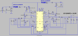
We have the attached 10.9A RMS current flowing in a 15A fuse.
Its at 450kHz.
The fuse is 2.16mm thick and surface mount.

Fuse part number is AF2-15.0V065TM

AF2-15.0V065TM Fuse

We calculated that the RAC/RDC is 5.1

Therefore the AC resistance of the fuse is 19.3mR (DC is 0.0038R)

As such, the power dissipation in it will be 2.9W.

Do you agree, this is way excessive. Do you agree, We must filter the current before it goes through
this fuse?
 
You measured Irms but not phase and assumed skin effect was the cause. I expect it is inductive (lossless) 6 nH which is expected with a 10mm wiggly fuse.

If you put a low ESR cap like 18 uF 1mohm the current will rise from a voltage source but the heat will be the same, so it won't be an effective fuse at 15A. Then you have to redesign your current limit protection.


I think if/when you figure out the reactance of traces for nH/mm and apply it to the SMD fuse, you will understand my simulation and correct your assumptions and improve your design.

1714702339052.png

https://tinyurl.com/ylvkbk2w SIMulation with Falstad circuits.

I used Saturn PCB toolkit to understand the 3D relationship of inductance nH/mm and pF/mm to make a quick estimate.

I recommend you define your design by specs, then choose a design to match.

e.g. Hall sensor to disable or use fuse before decoupling caps from supply or use a smaller fuse based on ESL and Rs or a thermistor, trigger/crowbar and a PTC.
 
Last edited:
How? There are no related informations in the datasheet.
Thanks, posts #27 and #33 of this...

with 450khz, x comes out as more than 10, so you just have to use the fact , as it says, that above x=3...the x vs k graph is a straight line, so you do the "y=mx+c" thing....and you get k = RAC/RDC = 5.1
 
You measured Irms but not phase and assumed skin effect was the cause. I expect it is inductive (lossless) 6 nH which is expected with a 10mm wiggly fuse.

(ignoring skin effect for now)
in a fuse you have a piece of fusing wire. This wire has a resistance R and thus resistive loss.
The loss is P = I_RMS * I_RMS * R.

Now if there is a stray inductance inside the fuse. It will mainly act in series with the R.
Thus for the fusing wire the loss still is P = I_RMS * I_RMS * R.

The voltage across the fuse may be different now, but since the power dissipation is the same ...
--> the fuse will trip at the same I_RMS. (with or withoout series inductance)

--> Load_side phase shift does not play a role for the fuse tripping point at all.

****
(now with skin effect)
But when we now consider a high frequency .. where the proximity effect comes into play ... the current in the fusing wire is more concentrated at the outer wire diameter.
The current is ont evenly distributed in the fusing wire.
The result is that the resistance of the wire increases at high frequencies.

Still the dissipation is P = I_RMS * I_RMS * R_s.
But now we have R_s = the resitance with skin effect included. R_s always is higher than R.

And thus the power dissipation is higher for high frequencies.
--> the fuse will trip at lower I_RMS. (at higher frequencies, where skin effekt plays a role)

****

Klaus
 
No idea how you are estimating skin effect here. Characteristic dimension is the wire gauge respectively film thickness of the fuse. I expect a thin-film fuse with < 50 um thickness.
 
Copper has a melting point just over 1000 °C. But the ambient factor is -25% derating for 100'C rise.
A -100% fuse current derating means the melting point is 25+400 °C at 0 amps.
1714727917382.png


The metal with a melting point of approximately 425 °C is lead (Pb) according to chatGPT but 327.5 'C according to Wiki with Cu melting >= 1085 'C which I think would cause toxic outgassing of epoxy so I might suspect it is more Bismuth+Cu+Sn allow with a low melting point and higher resistivity.

Yet the datasheet says the fusing element is "Copper or copper alloy composite fuse link" (?)


The PTC coefficient is 1.0039 is the +ve tempco. rate in Ω/°C times room temp R

Lead is only is also 1% higher PTC than copper but 12 times the resistance per cross-section area.

The R ratio at fusing temperature is 2.56 thus R(425'C)= 0.0038 * 2.56 = 9.78 mΩ. ref

For f= 450 kHz if sinusoidal has a skin effect of 98.4 um which is approx 3 oz copper thickness of copper but since the resistance ratio of R: {Pb/Cu} = 12 the tracks can be much thinner than fusing copper.

If the holding current is 15A then the holding power must be at least Pd = (Irms=15)² * R(425'C) = 225*9.78e-3Ω = 2.2 W

This temperature if conduct to the FR4 would burn the PCB and exceed the glass transition temp is much lower (150~ 180'C typ) but the fibreglass should prevent a sinkhole.
But you aren't far off in computing Pd by assuming skin effect is the cause, which is unknown due to the unknown inner trace thickness or how many layers.
You can prove your theory by making some measurements with variable f if you want.


Last words.

Upon reflection, I think the fusing material must be insulated inside the epoxy from the pad's solder temperature, otherwise it could tombstone off the pads.
We don't know the actual thickness and skin effective rise in resistance, and it may be significant but we do know the resistance will rise in temperature.
It does say a false trip may take up to 2 hrs to reset and 15A is the holding current not the trip current, so I don't think more than 2W is out of line for a fuse.

Perhaps you want to define your expectations in more detail and make more measurements to measure pad temps vs power dissipation and other factors that may affect reliability, OCP protection and false negatives vs false positives vs true positive protection.

Choosing the best solution depends mainly on your requirements, then test all the options by detailed tests and verifying it.
It is not trivial to test the reliability of fault detection and protection under all conditions of normal and abnormal environments.
You can certainly reach out to the factory tech support.

TY @KlausST I was wrong about using phase of RMS current which is the equivalent to DC current. B.F. '( The ESL may raise the voltage at 455 kHz if used as a current sensor for FET
 
Thanks, woops i forgot to post the actual fuse current waveform...

No idea how you are estimating skin effect here. Characteristic dimension is the wire gauge respectively film thickness of the fuse. I expect a thin-film fuse with < 50 um thickness.
Thanks, good point, i was taking the entire 2.16mm fuse thickness as doing the conduction and giving the 0.0038ohms
 
Last edited:
For 15A, it could be a matrix of series /parallel layers with conduction to convection air and SMD pads , lower e-resistance, skin effects & ESL inductance while raising thermal resistance but still fast enough trip time.

They've a TON OF PATENTS, so don't expect a rookie flaw.
 
re the waveform - it s rare to have real world current spikes like that - it assumes the rest of the connected ( driving ) circuit has very little wiring or stray inductance.

If you can, slowly increase the current thru the fuse and note the surface temp - ideally you should stay below 70 deg C

if this is not the case a square 4 of fuses may be necessary - or several in parallel.
--- Updated ---

SMT fuses are often not that fancy:
1714786452276.png


1714786514879.png

--- Updated ---

1714786635451.png
 
Last edited:
Initially, this thread is based on wrong assumptions and conclusions. Also the AC power dissipation calculation in post #1 is basically wrong.  If the fuse had an considerable amount of skin effect for 400 kHz square wave, you need to put in Rac for each harmonic component in the calculation and Rdc for DC component, not Irms and an average Rac. But the fuse element itself has probably no relevant skin effect, other circuit parts however have and are causing respective additional heating.

It's relative unusual to have a fuse in the switching current path of a converter. The points mentioned by Easy peasy should be considered (possible overvoltage during breaking, unwanted inductance). Without a schematic I don't even believe that the fuse serves a useful purpose.
 
Do you agree that the question can be improved?

False conclusions, missing data, is this real problem or a simulation

The skin depth of 0.5MHz on a printed copper trace is 100%.

After examining your plot
- the current spikes are from the capacitance ESR || RdsOn for all (I=V/R)
- the slope on square wave rising is the load inductance. nH/V = 500 approx from V = L * dI/dt
1714829517035.png


I don't know how they fit a 15A Cu fuse in a tiny SMD package but it is spec'd to rise 100'C at 75% of 15A ~ 11A which results in 39% rise in resistance for Cu.
I verified for my own satisfaction on Saturn PCB.exe and I agree that nobody else thinks there is any skin effect and ESL. Yet the FET also has a PTC effect like the fuse which Rs rises +39% for a 100'C rise which can lead to thermal runaway and fusing and maybe faster than the SMD fuse. It depends on a thermodynamics heatsink analysis for which you need to get specs and verify.

Protection & Power Delivery Network Design.
Unless you have specs. in mind for OTP or OCP, (protection from over-temp. or over-current) hypothetical questions like this should have some specs, assumptions & analysis. this includes I2t, packaging and environmental factors.

Although it is a creative idea to use a fast blow SMD fuse to protect a switching FET, unless you regulate the FET by some time limiter (e.g. PWM or disable), what's the point when there is no purpose, design specs or even logic diagram offered?

It would be more thoughtful in future to include all the details of your problem with assumptions and simulation and/or photo-layout of the realization.

This is how I would structure a question (more or less) in some logical sequence.

0. Problem statement or Executive Summary
1. Purpose of sub-system
2. Assumptions (what we need to know)
3. Design Specs (relevant subset)
4. Troubleshooting data
5. Analysis

Whereas for design the sequence is slightly different with Design for Testability DFT included with Design Specs and "unknowns" tested beforehand and Design Review and Verification Testing (DVT) as part of the design process.

A less useful question to assume you need to use some part and have a hypothetical issue with no purpose.

This is for others in a similar learning modes, to take this as constructive advice.

We all make misteaks, and the more you self-correct, gives you self-confidence and experience.
Solving problems early is a good thing, and there are better ways to save time for all of us.

Most errors are from wrong assumptions, simple over-sights and Murphy's Law.

How many watts does it take to blow a fuse? Actually
it is based on energy or I²t * Rs with PTC effects and thermal mass & insulation causing latency and loop gain of temperature towards melting point.
 
Last edited:
Thanks, its the well known and documented problem of high switching frequency Dual Sync Bucks both feeding into the same output.
Its 400W so you need to fuse the input.

Total Spec is 27vin, 13v5 out, 30A out, 450kHz. (2 interleaved bucks share this)

Max I(in) is 26.5A. You could use a single 30A fuse at the input, but above 15A, and DC fuses for up to 30V are expensive and scarce.
So, you have to use two fuses, one at the input to each sync Buck.

...then you run into the problem that each sync buck draws some of its input ripple current from the other sync Buck's input MLCC bank.....and
due to the two 15A fuses, this hideous ripple current ends up in these fuses...as the sim attached shows.
So , as is well known, L4 and L5 have to be added, as otherwise the fuses may have skin effect issues.....(though I am reading the kindly sent posts here to assess the thickness of the fuse's conducting element.)

Obviously, we would really like the 2 synch bucks to be both pulling from the same MLCC input capacitor bank...but due to the fact that they both have to be separately fused, with two fuses, each of half the current rating, we cant do this.
 

Attachments

  • SyncBuk _fuseSkinEffect.png
    SyncBuk _fuseSkinEffect.png
    93.3 KB · Views: 24
  • SyncBuk_Fuse skin effect.zip
    3.2 KB · Views: 19
Last edited:
Thanks, we have an inrush limiter, but because it doesnt help to demo this point here, of the 450khz square wave, i left it out.
 
skin depth ( mm ) is 0.066 / ( SQRT ( MHZ ) ), so for 35 um ( 0.035 mm ) pcb , at 450kHz the skin depth ( depth at which current density falls to 37% of surface value ) = 0.098 mm ( 98 um )

so anything similar in thickness to 1 Oz ( 35um / 0.035mm ) or 2 Oz ( 70 um / 0.07 mm ) will carry all the AC current without too many skin depth issues.

So I fail to understand - how you came up with your figures for AC resistance at 450kHz ? perhaps @cupoftea can illuminate for us ?
--- Updated ---

referring to the schematic - would it not be better to have the fuse directly adjacent to the top fet drain in each case ?
 
Last edited:
eferring to the schematic - would it not be better to have the fuse directly adjacent to the top fet drain in each case ?
Thanks, we are not sure how it is known that the 2.16mm thick fuse, has a conducting element that is only some 35um thick?. Its datasheet doesnt state this.
For the reason that we assume the full 2.16mm thickness is carrying the fuse current, we need to keep it with flat DC current in it.
 
Last edited:

LaTeX Commands Quick-Menu:

Similar threads

Part and Inventory Search

Welcome to EDABoard.com

Sponsor

Back
Top