Continue to Site

Welcome to EDAboard.com

Welcome to our site! EDAboard.com is an international Electronics Discussion Forum focused on EDA software, circuits, schematics, books, theory, papers, asic, pld, 8051, DSP, Network, RF, Analog Design, PCB, Service Manuals... and a whole lot more! To participate you need to register. Registration is free. Click here to register now.

Wrong measurement in dual-band power amplifier

Status
Not open for further replies.

dangan1993

Junior Member level 3
Joined
May 29, 2020
Messages
28
Helped
0
Reputation
0
Reaction score
0
Trophy points
1
Activity points
214
Hi everyone. I am a PHD student.
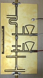
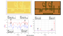
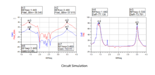
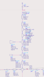
Currently, I try to design a dual band power amplifier at 1.4 and 3.5 GHz using CGH40006P transistor. I have gone to the last step of measurement with circuit shown in the attached picture, but my circuit just works well at 1.3 GHz and no gain appears in the high band. I see that my circuit has no problems in fabrication and just contains little lumped components as DC and bypass capacitors. Can someone give me recommendations to check as well as fix the problem. Thank you very much.
 

Attachments

  • BDAEC3FB-F299-4979-953A-964D2C600E3F.jpeg
    BDAEC3FB-F299-4979-953A-964D2C600E3F.jpeg
    400.4 KB · Views: 125

Have you ever simulated this circuit in EM simulator? Can you share the results with us??
How could you separate the bands?
 
Just looking to your PCB layout, I don't understand why you have different widths for the 50 ohms transmission lines.
OK, if a microstrip line is thinner than its width for 50 ohms, the line will behave as an inductance, but I don't think this was your intention in this design.
 
How good is the radial stub decoupling of supply lines at 1.4 and 3.5 GHz?
Layout looks like a narrowband solution, but these two frequencies are far apart.
 

As already pointed out in post #2, more detail are required to answer you question. For instance how did you designed the matching network, what about the substrate, ecc.
In any case its very difficult that a circuit at these frequencies, even if simulated, will behaves as expected without an on-board tuning.
If you are quite sure about your design, you should have a look at the gain (by means of a network analyzer using an attenuator on the output to protect the instrument) over the whole band, let's say from 1 to 4 GHz, to see if it could be mistuned.
Then you can use the small metallic tip of a plastic tuning tool to touch each single microstrip. Rather in general, if after touching the gain increases, then the line should by a little bit larger or a small capacitor (tenth of pF) has to be added, otherwise the line should by reduced. However this requires a good amount of experience in tuning RF boards.
Also the input and output impedences may play a role and should be measured. In this case be very careful because in measuring the output impedance the network could be damaged if an input signal is present (the input connector have to be terminated onto 50 ohms) or if the design is not stable a self-oscillation starts.
 
Have you ever simulated this circuit in EM simulator? Can you share the results with us??
How could you separate the bands?
Thank you for your reply. I had tried to perform EM simulation and the results are given below but it is so bad as compared to the circuit simulation-based results. I thought I have set up something wrong but I cannot find. "cry..cry"
--- Updated ---

Just looking to your PCB layout, I don't understand why you have different widths for the 50 ohms transmission lines.
OK, if a microstrip line is thinner than its width for 50 ohms, the line will behave as an inductance, but I don't think this was your intention in this design.
Thank you for your reply. I just insert 50-Ohm transmission line at each port of 50-Ohm for fabrication. I think it doesnt affect to the circuit operation.
--- Updated ---

How good is the radial stub decoupling of supply lines at 1.4 and 3.5 GHz?
Layout looks like a narrowband solution, but these two frequencies are far apart.
Thank you for your reply. Do you think the coupling effect between radial stubs and supply lines is reason??? But at low band, the performance is quite good. !!!
--- Updated ---

As already pointed out in post #2, more detail are required to answer you question. For instance how did you designed the matching network, what about the substrate, ecc.
In any case its very difficult that a circuit at these frequencies, even if simulated, will behaves as expected without an on-board tuning.
If you are quite sure about your design, you should have a look at the gain (by means of a network analyzer using an attenuator on the output to protect the instrument) over the whole band, let's say from 1 to 4 GHz, to see if it could be mistuned.
Then you can use the small metallic tip of a plastic tuning tool to touch each single microstrip. Rather in general, if after touching the gain increases, then the line should by a little bit larger or a small capacitor (tenth of pF) has to be added, otherwise the line should by reduced. However this requires a good amount of experience in tuning RF boards.
Also the input and output impedences may play a role and should be measured. In this case be very careful because in measuring the output impedance the network could be damaged if an input signal is present (the input connector have to be terminated onto 50 ohms) or if the design is not stable a self-oscillation starts.
Thank you for your useful recommendation. I have swept entire frequency range and the PA has gain of 13dB at 1.3 GHz. For high band, the gain is nearly zero. I use substrate TLY-5 (eps=2.2, 0.8mm). I have tried to perform EM simulation first, but the performance is so bad, as compared to circuit simulation-based one as in the attached file. Could you please recommend me about the EM setup? And Is EM simulation results always similar to or little worse than the circuit simulation results?? If we obtain so bad EM simulation results, what we should do next?
--- Updated ---
 

Attachments

  • EM_simulation.PNG
    EM_simulation.PNG
    173.7 KB · Views: 106
  • circuit_simulation.PNG
    circuit_simulation.PNG
    122.6 KB · Views: 108
  • substrate.png
    substrate.png
    189 KB · Views: 110
  • DualMode_PA_wrk.zip
    26 MB · Views: 99
Last edited:

Thank you for your reply. Do you think the coupling effect between radial stubs and supply lines is reason??? But at low band, the performance is quite good. !!!

I am not worried about coupling effects, but the fundamental design of your supply lines. Radial stub is something that we use for narrowband designs, and it looks wrong to me in this dual band context.

In circuit simulation you terminated them with an ideal voltage source at the EM pin/port, which creates an indeal short for all frequencies. You need to check real world response when adding much series inductance there to represent your DC supply lines. Does that have an impact on RF path response?

~~

Regarding bad results when looking at EM results: when used properly, EM results are more accurate than schematic models.

Looking at your ADS design, one big mistake is that you simulated microstrip models at schematic level (bottom ground only) but in layout you have top metal ground pour very close to all lines. That looks more like coplanar design, and will have a strong effect. If you want a layout that agrees with microstrip models, don't use ground pour on top metal!
 

Attachments

  • supply.png
    supply.png
    77.5 KB · Views: 102
I didn't go deep to measure the impedances vs line widths, and so on.
I assume the 34.12mil is the width of the 50ohms microstrip lines, but what is the reason using different widths (14.44mil and 18.95mil) at the input and output 50 ohms SMA connectors?
 

Attachments

  • layout.jpg
    layout.jpg
    333.7 KB · Views: 102
Volker is right. Since the whole bottom layer is ground, you don't have to define a second layer being as GND. Single layer and standard GND layer of Momentum is enough.
Distances are very close between microstrip elements and ground pour on TOP layer. You should clean around them. Otherwise, they will act as Co-Planar components.
 
I am not worried about coupling effects, but the fundamental design of your supply lines. Radial stub is something that we use for narrowband designs, and it looks wrong to me in this dual band context.

In circuit simulation you terminated them with an ideal voltage source at the EM pin/port, which creates an indeal short for all frequencies. You need to check real world response when adding much series inductance there to represent your DC supply lines. Does that have an impact on RF path response?

~~

Regarding bad results when looking at EM results: when used properly, EM results are more accurate than schematic models.

Looking at your ADS design, one big mistake is that you simulated microstrip models at schematic level (bottom ground only) but in layout you have top metal ground pour very close to all lines. That looks more like coplanar design, and will have a strong effect. If you want a layout that agrees with microstrip models, don't use ground pour on top metal!
Thank you for your comment. The radial stub is intended to be short at 1.4 GHz and the overall supply line is a Dual-Band Biasing network that means it provides open at both fundamental frequency band. An ideal voltage source can provide short at all frequencies, and it doesnt affect the fundamental matching. Because a RF choke with high inductance exhibits more loss and low impedance than a TLIN-based network at high frequencies, therefore I do not use in my circuit.
Regarding to EM results, I will try to do again, thank you very much.
--- Updated ---

I didn't go deep to measure the impedances vs line widths, and so on.
I assume the 34.12mil is the width of the 50ohms microstrip lines, but what is the reason using different widths (14.44mil and 18.95mil) at the input and output 50 ohms SMA connectors?
Thank you for your comment. 14.44mil and 18.95mil TLINs belongs to my matching networks at input and output. I just insert 34.12mil short-length TLINs for facilitating soldering and these short lines do not affect matching performance because source and load terminations are 50-Ohm.
--- Updated ---

Volker is right. Since the whole bottom layer is ground, you don't have to define a second layer being as GND. Single layer and standard GND layer of Momentum is enough.
Distances are very close between microstrip elements and ground pour on TOP layer. You should clean around them. Otherwise, they will act as Co-Planar components.
Thank you very much. I will try to do it again.
 
Last edited:

Don't zip the whole project directory as is, instead use "Archive Project" utility then zip this archived project to post here. And don't forget to include models (and other libraries) for forum users.
And use more appropriate organization for your project tree.
 
Don't zip the whole project directory as is, instead use "Archive Project" utility then zip this archived project to post here. And don't forget to include models (and other libraries) for forum users.
And use more appropriate organization for your project tree.
Thank you for your recommendation. I will do that.
 

Thank you for your comment. The radial stub is intended to be short at 1.4 GHz and the overall supply line is a Dual-Band Biasing network that means it provides open at both fundamental frequency band. An ideal voltage source can provide short at all frequencies,

Yes, but you don't have that ideal short there in real world hardware!
You really really need to check if your bias lines are properly decoupled with arbitrary impedance at that pin!
--- Updated ---


edit: I just checked using your schematic models: looks ok with both short and open.
 
Last edited:

Yes, but you don't have that ideal short there in real world hardware!
You really really need to check if your bias lines are properly decoupled with arbitrary impedance at that pin!
I understand your worry, but the dual-band biasing network is designed without being affected by any impedance the DC source brings. I also have added two bypass capacitors that can too yield short circuit at all frequencies.
 

I also have added two bypass capacitors that can too yield short circuit at all frequencies.

Yes, these 2.4nF are ideal in schematic simulation. Real world response at GHz frequencies is another topic ...

Good luck with your design!

Volker // Keysight Certified Expert EDA
 

Yes, these 2.4nF are ideal in schematic simulation. Real world response at GHz frequencies is another topic ...

Good luck with your design!

Volker // Keysight Certified Expert EDA
Yes, thank you for your kindness. ^^
 

I am not worried about coupling effects, but the fundamental design of your supply lines. Radial stub is something that we use for narrowband designs, and it looks wrong to me in this dual band context.

In circuit simulation you terminated them with an ideal voltage source at the EM pin/port, which creates an indeal short for all frequencies. You need to check real world response when adding much series inductance there to represent your DC supply lines. Does that have an impact on RF path response?

~~

Regarding bad results when looking at EM results: when used properly, EM results are more accurate than schematic models.

Looking at your ADS design, one big mistake is that you simulated microstrip models at schematic level (bottom ground only) but in layout you have top metal ground pour very close to all lines. That looks more like coplanar design, and will have a strong effect. If you want a layout that agrees with microstrip models, don't use ground pour on top metal!
Dear Expert, I have performed the EM simulation with cleared top medal ground but the results looks also so bad (cry..cry), which are shown in the attached files. Whether Is there any wrong setup for EM setup? Could you please give me some recommendations about that?
Thank you very much!
 

Attachments

  • DualClass_PA.zip
    32.6 MB · Views: 104
  • updated_EM_simulation.PNG
    updated_EM_simulation.PNG
    95.7 KB · Views: 107

Try again with your EM substrate modified so that bottom boundary is directly below the TLY substrate.

No layer names shown in my screenshot because your project references an external library that was not included. That also means we can't see your EM port layer definitions, and can't see if you defined your EM ports to use the explicit reference layer. By removing the bottom metal from EM stackup, we ensure that bottom boundary is used for port reference, and that should be perfect here because you have no cutouts in ground plane anyway.
 

Attachments

  • emsub.png
    emsub.png
    7.1 KB · Views: 101
Last edited:
Try again with your EM substrate modified so that bottom boundary is directly below the TLY substrate.

No layer names shown in my screenshot because your project references an external library that was not included. That also means we can't see your EM port layer definitions, and can't see if you defined your EM ports to use the explicit reference layer. By removing the bottom metal from EM stackup, we ensure that bottom boundary is used for port reference, and that should be perfect here because you have no cutouts in ground plane anyway.
Hi Volker, it works well. Thank you very much. For measurement, I think your first reason is true. The clearance in top layer make lines operate as coplanar waveguides. I will try to refabricate without clearance and measure again.!!!
Try again with your EM substrate modified so that bottom boundary is directly below the TLY substrate.

No layer names shown in my screenshot because your project references an external library that was not included. That also means we can't see your EM port layer definitions, and can't see if you defined your EM ports to use the explicit reference layer. By removing the bottom metal from EM stackup, we ensure that bottom boundary is used for port reference, and that should be perfect here because you have no cutouts in ground plane anyway.
 

Status
Not open for further replies.

Part and Inventory Search

Welcome to EDABoard.com

Sponsor

Back
Top