Welcome to our site! EDAboard.com is an international Electronics Discussion Forum focused on EDA software, circuits, schematics, books, theory, papers, asic, pld, 8051, DSP, Network, RF, Analog Design, PCB, Service Manuals... and a whole lot more! To participate you need to register. Registration is free. Click here to register now.
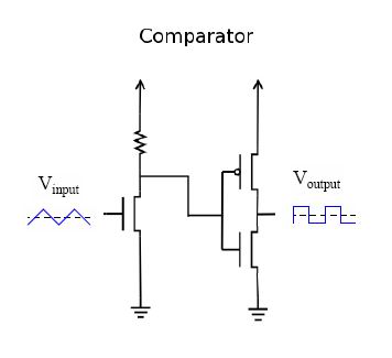
If you need to regard this as comparator, then the trip point is the inverter trip point where it can switch from L to H. Then first stage determines when to turn over when the INPUT is switching from VSS to some point (say, VDD/2) where parallel equivalent resistance of the RDS of NMOS and the up resistor is equal to the trip point of inverter, then the inverter turns from L to H, that's the comparison happens.
If you need to regard this as comparator, then the trip point is the inverter trip point where it can switch from L to H. Then first stage determines when to turn over when the INPUT is switching from VSS to some point (say, VDD/2) where parallel equivalent resistance of the RDS of NMOS and the up resistor is equal to the trip point of inverter, then the inverter turns from L to H, that's the comparison happens.
As we know that the trip point of a inverter is VDD/2, then in order to be the trip point voltage, the common source amplier effective dc voltage is designed at VDD/2. Then as the common source dc voltage increase or decrease from VDD/2 will trigger the inverter either to be in logic high or low.
This site uses cookies to help personalise content, tailor your experience and to keep you logged in if you register.
By continuing to use this site, you are consenting to our use of cookies.