Continue to Site

Welcome to EDAboard.com

Welcome to our site! EDAboard.com is an international Electronics Discussion Forum focused on EDA software, circuits, schematics, books, theory, papers, asic, pld, 8051, DSP, Network, RF, Analog Design, PCB, Service Manuals... and a whole lot more! To participate you need to register. Registration is free. Click here to register now.

why this Bicoms receiver test result is so large

Status
Not open for further replies.

xihuwang

Member level 2
Joined
Oct 23, 2007
Messages
46
Helped
1
Reputation
2
Reaction score
1
Trophy points
1,288
Activity points
1,595
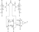
bicmos_receiver_gif.GIF

A Bicoms receiver design in a RS-485 tranceiver IC
speed requeriment : 50M bps
simulation result : 70M bps
But test result show , the transfer delay is 35ns , which is bigger than the spec and simulation result.

Can any one help me to analysis the reason ?

One of my guess is the PNP ( lateral pnp) current gain is small ,(about 30) , and has big B input resistance.
Lateral pnp can't be used in signal path . But we have no choice because another type pnp is substrat pnp.
Another guess is , the dc operation point is not in best condition .

Can any one give me your analysis on this circuit.

VD1 & VD2 are the inputs. The commo-mode region is -7 ~ 12V. The power supply is 5V.
The resistor network is uesed to transfer the -7~12V common mode region to the common mode
region of the transconductance stage.
 
Last edited:

did you run corner or montecarlo analysis? beta can be subject to large process variations

do you have control over bias currents of the input stage?
 

The simulation is the post layout simulation.
Under SS corner, VDD is decreased from 5V to 4.5V, Temp=125.
 

what about mismatch? do you have mismatch data for your bipolar devices, have you tried running montecarlo or estimating the mismatch and simulating with a simplified lumped mismatch? e.g. mismatching the current sources

you have not answered about control over the input stage currents

if you were to redo the design you should consider adding positive feedback for speed and noise immunity (hysteresis)
 

Why the mismatch affect the receiver's speed ?

What the mean " do you have control over bias currents of the input stage? "
 

A simple mechanism that would kill the speed of this input stage would be getting a bipolar out of its active region or a MOSFET out of its saturation region. Mismatch causes random offset, which can push your signal range outside the design region.

As of controlling the bias currents that would be to control the gm of your diff pair and perhaps compensate for offset if you can control individual currents in separate branches
 
Last edited:

It is not becautse of mismatch , I guess.
So what is the other reason.
 

Status
Not open for further replies.

Part and Inventory Search

Welcome to EDABoard.com

Sponsor

Back
Top