fencl
Member level 1
hi all.
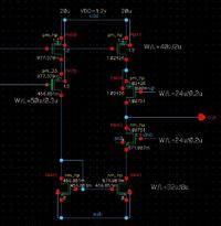
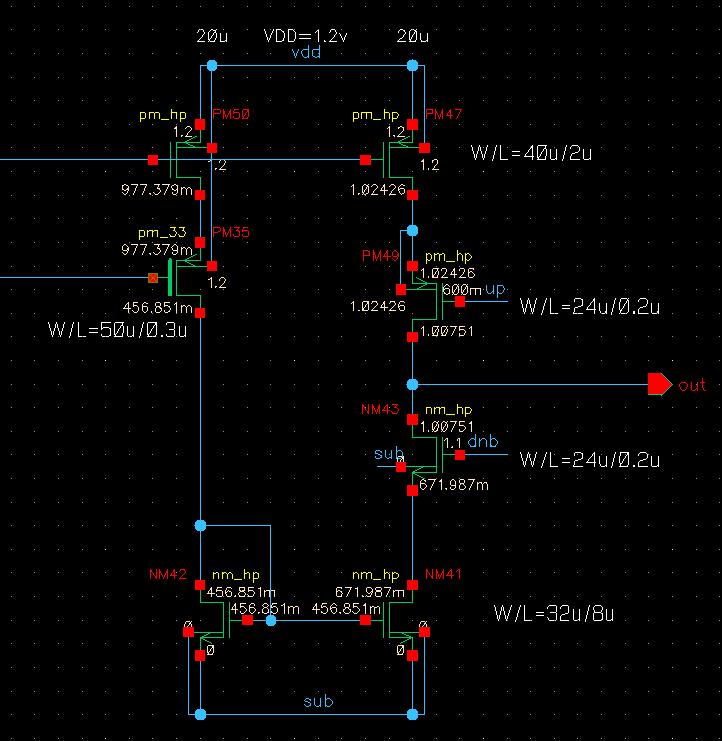
it's about chgpm op point for pll in 0.13um process. pm49 is in region 1.nm43 in region 3, while other mos all in saturation,only pm35 is 3.3v device.the supply is 1.2v. each path current is set to 20uA. the op point result is shown in image.
it seems pm49 appear small ron, why it's vds is so small compare to other device ,such as nm43 ?
since my Vout shoulb be around 0.7 when in op point.how can i do to achieve it? PM50,pm35 and pm47 is fixed why all other device and Vup and Vdnb cen be adjustl.
pls .....
 [/img]