Continue to Site

Welcome to EDAboard.com

Welcome to our site! EDAboard.com is an international Electronics Discussion Forum focused on EDA software, circuits, schematics, books, theory, papers, asic, pld, 8051, DSP, Network, RF, Analog Design, PCB, Service Manuals... and a whole lot more! To participate you need to register. Registration is free. Click here to register now.

why my sram cell does not store any value?

Status
Not open for further replies.

kpkp

Newbie level 6
Joined
Jan 27, 2012
Messages
12
Helped
0
Reputation
0
Reaction score
0
Trophy points
1,281
Activity points
1,358
Hi everybody, i'm making analog design of 6t SRAM cell in cadence. but my cell does not store the value 0 or 1 inside the cell. when i apply complementry values to bit line (Vdd) and bit_bar (gnd) line it keeps the value storing inside bt as i remove the voltage it takes the value of power supply. that means it does not store the values applied at bit line and bit_bar line...can anybody help me??? I have attached my schematic also herewith...
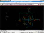
Screenshot-1.png
Thnx in advance...
 

I don't see any problem, in fact I am getting correct result in my simulation. I see nothing wrong except NM2 that is source and drain you can change. But That should not affect the result. Please check the models file if you have chosen correctly.
 
  • Like
Reactions: kpkp

    kpkp

    Points: 2
    Helpful Answer Positive Rating
Hello, thanks a lot for answer. I have solved the problem in writing operation. But now i am facing problem in reading operation. Actually i want to measure delay in read operation. so can you please help me in completing the read circuit??? I want to disconnect the data lines from cell while precharge voltage is on to charge the data lines. Therefore i have used tristate buffer which is disabled when precharge voltage is on , But I'm getting errors ... so can you please suggest me some changes or else? schematic has been attached herewith....
read2.png
Thanks in advance....
 

What the errors you get? This is just the logical implementation.
 

I got errors due to tristate buffer...Do you know how to configure the buffer or inverter ??
error says that netlist cannot be generated...
Thnks...
 

You can create your own tristate buffer. Try to use that. I prefer to use pass transistor gates for that.
 

yeah exactly. After that I have already tried pass transistor and i got the desired outputs...
but can you please tell me from which waveform I should measure the read delay? I mean to say from bit lines or from q and q_bar points? I have attached my waveforms here...Between 5 ns and 6 ns, when word line (WL) has been raised, the bit_bar has been discharged and bit line is still at high potential...so is it appropriate waveform to calculate the read delay?
read write.png
Thanks....
 
Last edited:

Status
Not open for further replies.

Part and Inventory Search

Welcome to EDABoard.com

Sponsor

Back
Top