Welcome to our site! EDAboard.com is an international Electronics Discussion Forum focused on EDA software, circuits, schematics, books, theory, papers, asic, pld, 8051, DSP, Network, RF, Analog Design, PCB, Service Manuals... and a whole lot more! To participate you need to register. Registration is free. Click here to register now.
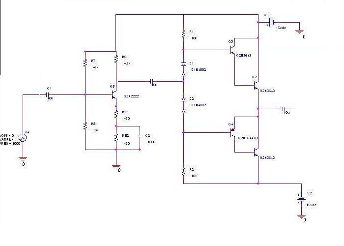
Fortunately Q4 has wrong polarity, otherwise Q1+Q2, possibly Q3 + Q4 would burn. The second stage can be
considered a suitable common emitter circuit, if you connect the output to Rc.
I don't know, where the output of 1st stage "must be connected" because I don't understand the circuit. I can't relate it
to a known amplifier principle circuit.
Wrong polarity means, that Q4 is not operating in active transistor mode. Check the polarity arrows.
Q4 looks like it 'should' be a compound PNP but the emitter and collector are reversed. However, I think you need to explain the rationalle behind the circuit. What are you trying to achieve? It seems a bit random.
I found, that the above circuits is simply reproducing the errors of a circuit previously posted by abbeyromy in the same thread.
If Q4 collector and emitter are exchanged, than it's working in principle.
As keith pointed out for the two transistor complementary follower at the top of this thread, the bias voltage is again too low,
so the circuit creates crossover distortions. Three or four diodes should be used.
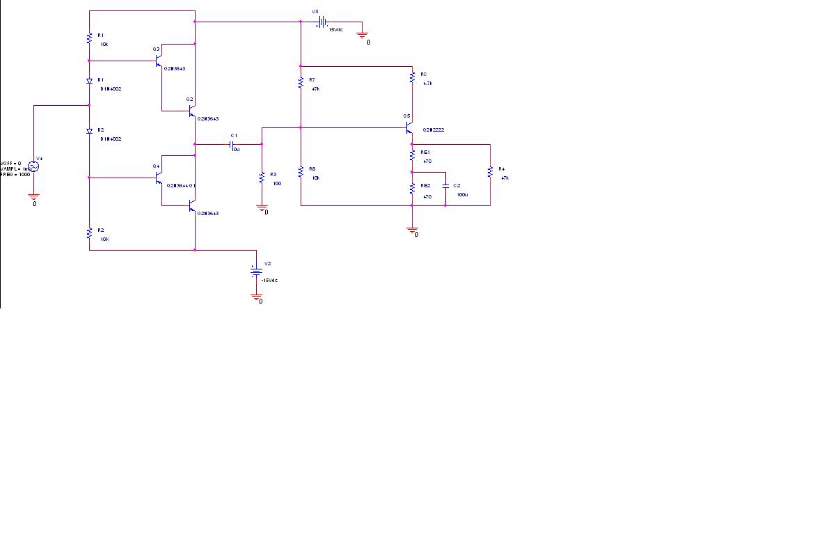
The purpose of the overall circuit seems dubious. One would expect the common emitter stage to be connected as a preamplifier and
the complementary follower as output stage. To achieve a gain > 1, the output stage must be connected to the collector of Q5.
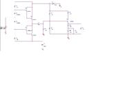
P.S.: I think, the overall structure should look like this:
actually, i am trying to compare the circuit performance on different classes of power amplifier..
i have try worked on different classes of power amplifier..yup,the circuit quasi complementary is provided by abbey..
my problem is i have designed the power amplifier of class b and ab..but the output do not amplify..
i have post my schematic previously...
I don't see open question with the said circuits. It has been clarified, that the "follower" circuits have a voltage gain ≈ 1
(but a considerable current and power gain). A common emitter amplifier circuit as above can provide the voltage gain. Both
circuits have no particular problems, if implemented correctly (reasonable dimensioning, placing the transistors correctly,
connecting all circuit nodes).
As a not yet addressed topic, you may want to include the output stage in an overall feedback loop to reduce distortions.
You hardly won't find an audio amplifier without feedback in the output stage. But it's not required for basic operation, you can
think of it, if the basic circuits started working for you.
i need to analyze the basic operation of power amplifier class B.. in your opinion..,can i just choose the class B part without combining the circuit with common emitter?
This site uses cookies to help personalise content, tailor your experience and to keep you logged in if you register.
By continuing to use this site, you are consenting to our use of cookies.