Continue to Site

Welcome to EDAboard.com

Welcome to our site! EDAboard.com is an international Electronics Discussion Forum focused on EDA software, circuits, schematics, books, theory, papers, asic, pld, 8051, DSP, Network, RF, Analog Design, PCB, Service Manuals... and a whole lot more! To participate you need to register. Registration is free. Click here to register now.

Why frac N's phase noise is worse than int N about 10dB?

Status
Not open for further replies.

wyhgod

Newbie level 4
Joined
Sep 5, 2008
Messages
5
Helped
0
Reputation
0
Reaction score
0
Trophy points
1,281
Activity points
1,332
Dear all,
I have designed a fractional N synthesizer,and multi-modulus N range is from 64-255.Using 20 bit sigma-delta to implement fractional mode.
Power supply for multi-modulus N and sigma-delta are bonding to pad seperately,and are 3.3v.

when i test close loop phase noise, i find the phase noise in int N mode is better than frac N mode about 10dB(@10khz,@100khz),both modes use the same N.

In frac mode,when i reduce power supply voltage for multi-modulus N to 2.2V ,the phase noise is better about 5db than 3.3v power supply for multi-modulus.
Also in frac mode, if i reduce power supply voltage for sigma-delta, there is no change for phase noise.

first question,why is there 10dB phase noise difference between INT N mode and frac N mode.
second question,why the pahse noise is better if i reduce power supply voltage for multi-modulus N.
Can anybody tell me why?

Best Regards
devin
 

If I understand, you are using the exact same chip, but are programming it so that you use only integers for one setting, and then you change so you are using some fractionality? Like N goes from 1000 to 1000 1/32? Should be pretty much the same phase noise. What you want to check is that the phase detector frequency is the same in both cases!

The spurs might get worse with fractional programming.

I suspect that somehow you are using very different divisor ratios, even though you think they are almost the same. Are you using some canned laptop program to set the registers, such as AdiSimPLL?

Try downloading the exact registers binary used for the two cases, and see if they vary significantly.

As for lowering the voltage....it should make things worse, not better!
 

Thanks very much.you are the first one to reply this post.
yes,i use the exact same chip, first i make it lock in integer mode,then i just turn on sigma-delta,and find the phase noise is worse.
I am quietly sure that phase detector frequency is the same in both cases! because the locked frequency in both cases is right.
Also i think lowering power supply will make things worse, it is really very strange.

All digital grounds and digital power supplys are connected together,including dual modulus divider,M counter ,A counter, PFD and sigma-delta on chip.
i doubt that some analog blocks are interfered by sigma-delta.

Does anybody meet this case before?
i will appreciate very much if someone can help me to solve this problem.
 

a gps chip, pll provides LO frequency for receiver and PLL is integrated on the chip with receiver.
 

If it is some type of custom chip, then all bets are off. Maybe the switch in more circuitry with a poor noise floor when you turn on the signa-delta.
 

Devin

don't worry, you are facing the same issues that each designer found out starting playing with sigma delta rf synthesizer.

Those guys are bad. Really bad (I'm playing of course). In your case maybe the issue is not so high as gps specifications are quite relaxed for phase noise.

The question you put here is probably a quite complex one, and a dedicated consulting should be needed, I guess. But let's start from the beginning and try to clear some points:

1. Do you have a reliable (linear) model of your integer-N PLL that fits the measurments (so you include there VCO noise, reference noise, charge pump noise, prescaler noise, KVCO and so on)? Could you share us a plot with comparison of the simulated noise and measured noise?

2. Could you share some info about your IC? Loop filter is integrated? What test signals have you forecasted?

3. Did you measured the boundary spurs (for example if PFD frequency is 26 MHz and N=61.001 you'll have a LO at 1586.026MHz and a spur at 26 kHz from the carrier that won't be filtered by loop filter (I'm assuming you are using a loop bandwidth larger that 26 kHz, commonly used in sigma delta synth to minimize integrated phase noise)?

4. Are you aware about the charge pump linearity effects in sigma delta noise?

These aspects are related to theory & simulations and a good design should have all under control. But generally the most critical one are related to:

1. Supply connection: noise (in particular switching noise in CMOS dividers, reference path, PFD and charge pump) can couple through supply to VCO and analog parts
2. Substrate isolation and layout floorplan: if your design is for some mobile application you're probably doing it in submicron CMOS (65 nm?) and those processes have low substrate resistance, no trench. A proper floorplan is mandatory.
3. Bonding diagram and proper PCB decoupling

As I told you from the beginning it could be difficult to solve this issue only from a forum discussion, at least we are trying.

Mazz
 

Hi Mazz,
Thanks for your advice very much. The technology i use is 0.35um BiCMOS.
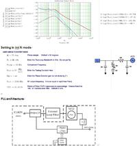
I use mathcad to model closed loop phase noise.
vco frequency is 3390.84MHz , lo frequency is 1695.42MHz,and div2 is in loop.

the following noise is simulation result.
PFD+CP output noise
Frequency OutNoise nV/rt.Hz HB db
10 5.50E-01 -9.26E+01
100 1.80E-01 -9.74E+01
1.00E+03 6.00E-02 -1.02E+02
1.00E+04 3.00E-02 -1.05E+02
1.00E+05 6.00E-03 -1.12E+02
1.00E+06 7.00E-03 -1.12E+02
1.00E+07 6.00E-03 -1.12E+02
1.00E+08 1.00E-03 -1.20E+02

VCO phase noise
Frequency OutNoise dbc/Hz (PSD)
1.00E+03 -44.58
1.00E+04 -78
1.00E+05 -100
1.00E+06 -120.4
1.00E+07 -140.7
1.00E+08 -160.4

Reference noise
Frequency OutNoise db/Hz nV/rt.Hz
1 -90 3.16228E+04
1.00E+01 -120 1.00000E+03
1.00E+02 -130 3.16228E+02
1.00E+03 -145 5.62341E+01
1.00E+04 -154 1.99526E+01
1.00E+05 -158 1.25893E+01
1.00E+06 -158 1.25893E+01
1.00E+07 -158 1.25893E+01
1.00E+08 -158 1.25893E+01

Test and simulation result:
Freq offset Turn on Sigma-delta Turn off Sigma-delta Int N Simulation result unit dBc/Hz
(@1695.42MHz) (@1690MHz) (@3390MHz)
@1kHz -79 -83
@10kHz -74 -81 -82
@100kHz -91 -100 -97
@1MHz -112 -127 -120

I didn’t record boundary spurs, I will attach the spur test result when I get it.
Also, I didn’t pay much attention to charge pump linearity effects in sigma delta noise.
I will try what you have told me.


---------- Post added at 07:44 ---------- Previous post was at 07:40 ----------

the image i attached contains closed loop phase noise simulation results,loop setting and PLL architechture.
 

It is interesting, a GPS in 0.35um BiCMOS, is it for some R&D project or it has application in some product? Today new GPS design are done in deep submicron CMOS when integrated with other systems or with baseband IC for mobile applications.

What I see here is that you're following the common way to do this design. You should include in some way in the linear model the noise coming from the sigma delta, at least to be sure to filter the normal bump it will generate around 5-10MHz (in your case).

About charge pump linearity effects there should be some literature in IEEE, take a look there, you'll find some paper if I remember well.

A suggestion could be to try to improve the quality of the model making a nonlinear model. I have seen (but not used) the tool done by Perrott, Cppsim (CppSim System Simulator)

It is free and can give you a good advantage in simulation of the overall performance.

I hope it can help.

Mazz
 

    V

    Points: 2
    Helpful Answer Positive Rating
Thanks for your advices again.
i just use 0.35um BiCMOS to verify some thoughts.
i will try what you have told me .
 

Status
Not open for further replies.

Part and Inventory Search

Welcome to EDABoard.com

Sponsor

Back
Top