Continue to Site

Welcome to EDAboard.com

Welcome to our site! EDAboard.com is an international Electronics Discussion Forum focused on EDA software, circuits, schematics, books, theory, papers, asic, pld, 8051, DSP, Network, RF, Analog Design, PCB, Service Manuals... and a whole lot more! To participate you need to register. Registration is free. Click here to register now.

Why does metal2 shold be vertical ?

Status
Not open for further replies.

amitjagtap

Full Member level 5
Joined
Jan 10, 2007
Messages
304
Helped
42
Reputation
84
Reaction score
36
Trophy points
1,308
Activity points
3,273
hi all,
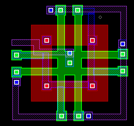
Why does metal 2 should be in vertical and metal 1 in horizontal direction?
Is it neccessary that circuit layout should satisfy this criterian?
Plz, Help me out.
 

No, it is not necessary.
I think this kind of layout is to reduce the magnetic interference and crosstalk between two kinds of metals
 

Routing can be in any direction you like. The main reason for doing metals in oppostite directions is to make your life easier when routing, it looks neat and saves time.
 

In my layout i'm using advanced layout structure for mirror to reduce mismatching between ttransistors. In that stucture it is difficult to single metal. and thus metal2 is used, which is not vertical.
 

k_90 is right... this is just a technique in designing. it is not really a requirement.

k_90 said:
Routing can be in any direction you like. The main reason for doing metals in oppostite directions is to make your life easier when routing, it looks neat and saves time.
 

amitjagtap said:
In my layout i'm using advanced layout structure for mirror to reduce mismatching between ttransistors. In that stucture it is difficult to single metal. and thus metal2 is used, which is not vertical.

the answer from K-90 is the root cause. in your case, you can change the rule based on your requirement.
 

It's not a requirement at all, but when you are designing a complete chip and you need to route toplevel signal lines you'll need a neat and ordered routing both in the chip toplevel and the lower hierarchy blocks to make your life easier and get things done on time...
 

Hi,
It is not necessary that you should not route M2 vertical.

You can route in horizontal also.

But if you route one metal in one direction only then it will
be easy for you the routing .Other wise later on you may get stuck in routing

basic idea is route all odd metal in one direction & even metal in other direction.

Regards,

Analayout.
 

it's not always vertical but it looks better and easy to route. but if not doing so will compress the area then that's better as long as matching is not affected.
 

The number of metals available in your process determines how you design your cell. If you have five or six layers of metal, then you have a lot of freedom to wire the way you want. In our grid-based approach, you might say, “Ok, Metal One will run horizontally and we’ll run power on Metal One. Metal Two runs vertically, Three horizontally and Four vertically.” Some people might only run power on Metal One. Some might decide to run power on Metal Five. You have
all the latitude and creative discretion you desire if you have that many metal layers to work with.
 

I think that it is kind of thumb rule to keep orientation of metals some how. For example in a 4 metals, I am trying to keep met1 and met3 on a direction (no matter vertically or horizontally) and met2 and met4 on the other. In this situation, practically I can easily inter-connect my metals and I also avoid possible routing congestions or blocked routing channels.
 

metal routing direction doesn't mean you have to comply with them...but for easy connection it's a rule of thumb in doing layout that you have at least a rule to follow...for instance all odd metals be routed horizontal and even metals vertical or vice versa.
 

Appreciate all.
Most of the statements above are excellent.

OK, there is a reason for alternate orientation switching - in other words - We intend not to run neighboring routed metal wires having long parallel run. And the reason is reduction of parasitic cap coupling across layers. In better terms - orientation switching - leads to distribution of parasitic capacitors [ which is way better than what would be otherwise ]

Metal(n) should not have long-run parallel area overlap with Metal(n-1) or Metal(n+1) - That helps Timing and Signal Integrity.

In 90nm and below - not only capacitor coupling - Mutual inductive coupling is another major threat.
 

sat said:
Appreciate all.
Most of the statements above are excellent.

OK, there is a reason for alternate orientation switching - in other words - We intend not to run neighboring routed metal wires having long parallel run. And the reason is reduction of parasitic cap coupling across layers. In better terms - orientation switching - leads to distribution of parasitic capacitors [ which is way better than what would be otherwise ]

Metal(n) should not have long-run parallel area overlap with Metal(n-1) or Metal(n+1) - That helps Timing and Signal Integrity.

In 90nm and below - not only capacitor coupling - Mutual inductive coupling is another major threat.

That's right the goal is to minimize the area of face to face metal in order to reduce the coupling capacitance.
 

Its actually needed in physical design where the toll does the routing.... we use metal 2 vertically so the tool algorithm is much more efficient ..
 

you can route in any metals in any direction, normally people change the direction of altrenate metal routing to make life easier while doing PNR (Palcement and Routing) with tool. But really helps a lot to reduce parasitics in high speed and analog IC design.
 

Q. Should m2 be vertical?
A. It depends.

The protocol established by your organization is usually what determines this.

Here ia a basic explanation of metal direction requirements.

As a rule layout design routing is best organized by alternating each subsequent metal layer from the lowest to the highest. Adherence to this protocol generally provides an unobstructed grid for routes to travel across the silicon through the available desired metal layer. Changing to adjacent (upper or lower) metal layers is simplified because of the available intersection opportunities assured by the protocol.

It is not uncommon to see m01 vertical as the starting orientation. This would then set the subsequent directions as follows:

vertical: M01, M03, M05, M07, M09, etc.
horizontal: M02, M04, M06, M08, M10, etc..

Or it can also be the opposite, (neither is right nor wrong):

horizontal: M01, M03, M05, M07, M09, etc.
vertical: M02, M04, M06, M08, M10, etc..

Hope this helps.
 

its not necessary to routing the M2 in veirtically only.... it depends on rouuting complexity and no of metals avallaable...
 

Status
Not open for further replies.

Part and Inventory Search

Welcome to EDABoard.com

Sponsor

Back
Top