rashipatel
Newbie
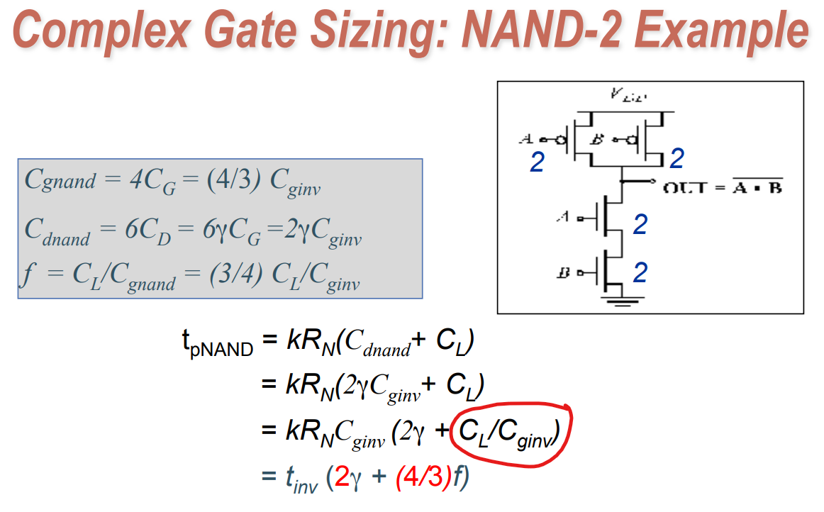
According to the below derivation:
Electrical effort is shown as CL/Cginv.
Cginv term is coming because of Cdnand term. If we connect an external load Cin to the gate of this nand circuit, it will not be related to Cnand in any manner as according to the information given gamma is technology dependent, so I am assuming its related to the parameters of the gate and would not depend on external loads. Please help me clear the confusion here.