Continue to Site

Welcome to EDAboard.com

Welcome to our site! EDAboard.com is an international Electronics Discussion Forum focused on EDA software, circuits, schematics, books, theory, papers, asic, pld, 8051, DSP, Network, RF, Analog Design, PCB, Service Manuals... and a whole lot more! To participate you need to register. Registration is free. Click here to register now.

why cannot High Side IGBT Driver pull the gate to zero Volts while PWM is Off ?

Status
Not open for further replies.

anotherbrick

Full Member level 4
Joined
Jan 10, 2009
Messages
217
Helped
1
Reputation
2
Reaction score
1
Trophy points
1,298
Location
Istanbul , Turkey
Activity points
3,144
hello dear forum

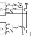
I build a high and low side driver
with HCPL 3120 ( 2 Amps sink source ) optocoupler it is in this picture
bootstrap.JPG

the bootstrap cap is 1 uF
( the reverse diode paralel to gate resistor is there but not shown in the picture )

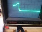
my question ; why cannot the high side pull the gate signal down to 0 V when the high PWM is Off ?

see this picture
high side osciloscope view.JPG

thank you
 

Waveform is about to useless without voltage and time scale.

How did tap the voltage? Differential probe? Are you sure the waveform shows true highside Vgs?
 
Hi,

It simply is not necessary to drive the high side gate to GND.
The driver just connects gate with source to get about zero V_gs. This shuts OFF the Mosfet.
For example if both gate and source are 12V then the Mosfet is OFF.

If you want the source voltage of the high side Mosfet to be zero, then you need to switch ON the low side Mosfet.
Then the bootstrap diode can charge the bootstrap capacitor.

Klaus
 
Last edited:
High side driver can only pull high side gate to high
side source. Maybe the low side driver's Vce(sat) is
the limitation - high side source sits on that.
 
Hi,

Thanks for pointing out that I've mixed "source" and "drain".
I've corrected my post above.

Klaus
 
hello dear forum members,

I measured high side Vgs with normal osciloscope probe - I used isolated transformer for powering osciloscope

the time base is 4 microsec / div - voltage base is 5 V / div - the PWM signal is 28 KHz

the IGBT is 100 A / 600 V dual modul

the signal is taken when the inverter runs at 2 Amps mains load

how can I pull high side Vgs to zero when the High-PWM signal is "0" ?

thank you
 
Last edited:

sorry I used wrong words - I am not native english speaker
I corrected my message

please look at the osciloscope photo attached to 1st message

I draw a yellow arrow for pointing to my problem - I want this residue voltage go away

thank you

PS. I am already switching low side ON
 

Hi,

then I assume you see just see the deadtime between HIGH_SIDE_OFF and LOW_SIDE_ON (about 800ns).

I think there is nothing wrong with your wavefrom. No need to change anything.

Klaus
 
I measured high side Vgs with normal osciloscope probe - I used isolated transformer for powering osciloscope
Hopefully the method doesn't distort the waveform.

Regarding the marked step in the waveform, it might occur during Vce rising edge caused by reverse transfer capacitance. We need to see the related Vce waveform. It would be also interesting to see the difference between driver output and gate voltage.

I wonder if a 100A IGBT should be used with negative gate voltage?
 
The Rext will limit the gate voltage to higher than 0 during switch off, other than that it is easy to have measurements during switching that are not entirely accurate dus to dv/dt upsetting the scope etc...
 
Status
Not open for further replies.

Part and Inventory Search

Welcome to EDABoard.com

Sponsor

Back
Top