Continue to Site

Welcome to EDAboard.com

Welcome to our site! EDAboard.com is an international Electronics Discussion Forum focused on EDA software, circuits, schematics, books, theory, papers, asic, pld, 8051, DSP, Network, RF, Analog Design, PCB, Service Manuals... and a whole lot more! To participate you need to register. Registration is free. Click here to register now.

what the max current value for the die bump to package ball connection (through via)

Status
Not open for further replies.

R1kky

Junior Member level 3
Joined
Nov 3, 2011
Messages
27
Helped
1
Reputation
2
Reaction score
1
Trophy points
1,283
Activity points
1,454
Hello, does anybody can advise what restrictions for current through vias of package substrate and so on for the bump-ball interconnections?

what parameters influence on this (max current) value (material, thickness?)?

apreciate your help.

- - - Updated - - -

as i understand there are next vias type
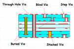
Vias.png
 

As you correctly state, bump-ball interconnection resistance depends - apart from the vias' resistance - on material and bump diameter. Generally one can say, bump connections are thicker and shorter than comparable wire bond connections: e.g. a 25µm thick and 1mm long gold wire can be used for up to 400mA. A 75µm diameter gold bump on the same pad size of course is much shorter (50 .. 100µm) and its heat transfer is much better, so could stand a lot more current (order of ampères).

In such case, the current more likely is limited by the vias' resistance, I think.
 

Status
Not open for further replies.

Part and Inventory Search

Welcome to EDABoard.com

Sponsor

Back
Top