sjamil02
Member level 4
- Joined
- Nov 8, 2009
- Messages
- 72
- Helped
- 9
- Reputation
- 18
- Reaction score
- 5
- Trophy points
- 1,288
- Location
- United Kingdom
- Activity points
- 1,961
Hi All,
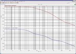
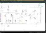
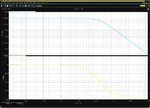
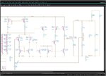
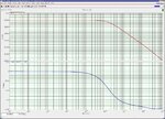
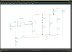
When I simulated the loop gain and phase margin (See attached schem for sim setup), the simulation results look's strange. How to measure phase margin from the plot? Is the simulation result correct? If not, how to get the correct result?
Note: The circuit is shunt regulator and I did not put compensation capacitor yet. For the loop gain setup, L=1mH and C=100uF.

")