Continue to Site

Welcome to EDAboard.com

Welcome to our site! EDAboard.com is an international Electronics Discussion Forum focused on EDA software, circuits, schematics, books, theory, papers, asic, pld, 8051, DSP, Network, RF, Analog Design, PCB, Service Manuals... and a whole lot more! To participate you need to register. Registration is free. Click here to register now.

Using the LTC4054 charging IC But it heats up a lot .

Heena09

Junior Member level 3
Joined
Jan 21, 2022
Messages
28
Helped
0
Reputation
0
Reaction score
0
Trophy points
1
Activity points
215
Hi every one .

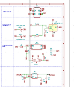
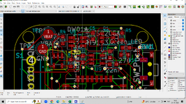
For the battery charging circuit, I used LTC4054 from an analog device. And its working fine but more heat dissipation is there and due to that, sometimes the chip is damaged. We tested Current rating and change it as given in datasheet for 450 mA current for charging.

But when we used the wall mount adapter, the chip heated more than the regular one. And the battery specification is 3.7V, 500mAh only.

Please guide me .

https://www.analog.com/media/en/technical-documentation/data-sheets/405442xf.pdf
 
Hi,

it is a linear regulator, thus thermal dissipation is quite normal and can be calculated with P_tot = (V_in - V_out) * I
If the chip gets damaged ... then (forgive my clear words) you have done something wrong.

Now we currently don´t see what you have done, thus we are unable to help you.

So show your schematic, your PCB layout and some photos of your wiring (100kBytes each is sufficient).

Klaus
Hi,

Thank you ,

Here I am sharing the schematic. Here we have a wall adapter for charging and an LDO for regulated output to the rest of the system . DW0 and FS8205A are battery protection ICs.

It's a very simple one but why is this LTC heated? We can't figure it out. especially one and some time it damages the battery too.
 

Attachments

  • BMS+LDO.png
    BMS+LDO.png
    15 KB · Views: 49
Hi,

no answer without PCB layout and photos.

And on the given schematic I can not read part values and signal names.

Klaus
 
Hi,

the reason is as simple as consistent.
Sorry for being direct. Please see my feedback not as rude, but rather like the error report of a software compliler

I asked for Schematic, PCB layout and photos. .. Only the PCB layout is something we can use. The other ones are still missing.

The datasheet has a chapter about thermal considerations --> you did not follow the datasheet recommendations
The datasheet has a chapter about stability --> you did not follow the datasheet recommendations
There is a design note .. the same
There is a demo board with documentation .. which also shows all the layers of the PCB layout ... again the same

I mean: the manufacturer provides all information. Does a great job to support designers. They literally did the whole PCB layout for you.
But if you ignore all this informations ... you can´t be surprised that it does not work properly.

***
Now you ask to be guided. How can I guide you? What other/new information do you need that is not already provided by the manufacturer?

I could read the documents for you ... I could copy_and_past the texts here ... then still you have to read the posts here and do your design accordingly.
Example:
* datasheet --> Thermal considerations -> Table 1 --> 2500mm^2 copper area (1 Oz copper) ... where is this 2500mm^2 copper area on your PCB?
* datasheet --> Pin Functions --> VCC (Pin 4) --> 1uF bypass capacitor ... where is it on your PCB?

***

The only thing I miss in the datasheet / design files: Is the recomendation to place the Vcc capacitor as close as possible to the IC .. with low impedance connections.
But this is a very general rule for all ICs and all designs .... mayby thus they think it does not need to be mentioned anymore.

A solid GND plane is mandatory here, because of two reasons: For signal/power reference stability and to spread the heat ...


Klaus
 
Also please expand on "But when we used the wall mount adapter, the chip heated more than the regular one.".
What do you mean by "the regular one" and what is the output rating of the wall mount adapter. As already pointed out, in a linear regulator the heat dissipated is proportional to the voltage dropped ACROSS it and the current THROUGH it. Even if the current is regulated, putting more voltage in to get the same voltage out means more voltage is dropped across it and hence more heat.

Brian.
 

LaTeX Commands Quick-Menu:

Similar threads

Part and Inventory Search

Welcome to EDABoard.com

Sponsor

Back
Top