Rajinder1268
Full Member level 3
Hi,
I have attached a part of the datasheet for a FTDi device.
The evaluation schematic board has a filter and 10nF connected between VBUS1 and 0V. I can't see the point of the filter as VBUS1 is connected directly to the FTDI chip (pin 12)?
The FTDI hardware recommendations state there is a different filter configuration. This makes more sense as the VBUS is filtered to obtain a clean 5V0 supply that would then power the FTDi chip.
Do I need to include the first schematic (ferrite + 10nF) and then from the ferrite/10nF junction add the second schematic for additional filtering i.e. 10nF + ferrite (BK0) + 100nF + 4.7uF?
Which one do I use or is it a combination of both?
Thanks in advance.
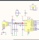
I have attached a part of the datasheet for a FTDi device.
The evaluation schematic board has a filter and 10nF connected between VBUS1 and 0V. I can't see the point of the filter as VBUS1 is connected directly to the FTDI chip (pin 12)?
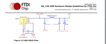
The FTDI hardware recommendations state there is a different filter configuration. This makes more sense as the VBUS is filtered to obtain a clean 5V0 supply that would then power the FTDi chip.
Do I need to include the first schematic (ferrite + 10nF) and then from the ferrite/10nF junction add the second schematic for additional filtering i.e. 10nF + ferrite (BK0) + 100nF + 4.7uF?
Which one do I use or is it a combination of both?
Thanks in advance.
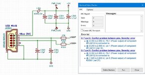
") . Please provide the corresponding sketch.
. Please provide the corresponding sketch.