Continue to Site

Welcome to EDAboard.com

Welcome to our site! EDAboard.com is an international Electronics Discussion Forum focused on EDA software, circuits, schematics, books, theory, papers, asic, pld, 8051, DSP, Network, RF, Analog Design, PCB, Service Manuals... and a whole lot more! To participate you need to register. Registration is free. Click here to register now.

Ucc2813-0 & ucc28c43d

Status
Not open for further replies.

wei9321

Member level 3
Joined
Feb 5, 2009
Messages
55
Helped
0
Reputation
0
Reaction score
0
Trophy points
1,286
Activity points
1,609
Ucc2813-0 & ucc28c43d question

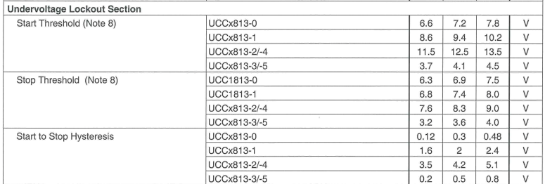
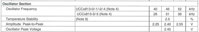
ucc28c43 & ucc2813-0 datasheet as the fllowing:
**broken link removed**

1.as fgure 1.what does it mean in the figure 1's BLOCK DIAGRAM ?
77_1298880117.jpg

figure 1
2.as figure 2,the vref pin and Ct/Rt pin connect capacitor and resistor can generate a triangle wave,why ?
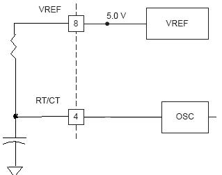
70_1298880064.jpg

figure 2
3.as figure 3,is the opa a comparator?
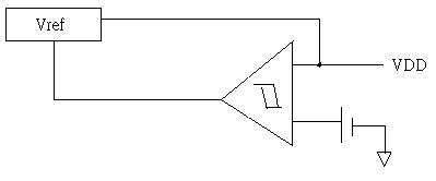
62_1298879989.jpg

figure 3

thanks!
 
Last edited:

https://focus.ti.com/lit/ds/symlink/ucc2813-2.pdf

The upper section indicates the under voltage lock out section. VCC is compared to a voltage by a comparator with hysteresis. It has to rise above a given level before the reference, and the rest of the IC is enabled. When it falls below the lower level the reference and IC is disabled.


In the middle section RT from VREF charges CT to some peak value, 2.45V, at which point circuitry in the block labelled OSC discharges it to some lower level, 50mV.


Next the upper device is a comparator with hysteresis, the lower one is a comparator without hysteresis.

Leading edge blanking disables/blanks the current limit comparator for 100nS when the output drive rises. This is to ignore any initial spikes on the current sense signal during switch turn on.


Genome.
 

Status
Not open for further replies.

Similar threads

Part and Inventory Search

Welcome to EDABoard.com

Sponsor

Back
Top