Continue to Site

Welcome to EDAboard.com

Welcome to our site! EDAboard.com is an international Electronics Discussion Forum focused on EDA software, circuits, schematics, books, theory, papers, asic, pld, 8051, DSP, Network, RF, Analog Design, PCB, Service Manuals... and a whole lot more! To participate you need to register. Registration is free. Click here to register now.

TXS0104E level shift input oscillation

Status
Not open for further replies.

james.qiu

Newbie level 6
Joined
Dec 25, 2021
Messages
11
Helped
0
Reputation
0
Reaction score
0
Trophy points
1
Activity points
145
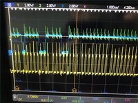
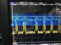
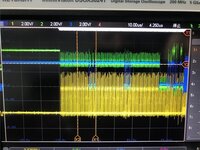
Hello , when i use TXS0104E , B port is 5V signal, A port is 3.3V, signal is SWD data with 10k external pull up resistor , the problem is when try to connect the j-link with 4Mhz,the data signal (port B)is clamping to 3,3V, then oscillation ,finally clamping to 2V at low voltage. i also try the nxp NTS0104PW , it is no problem, jlink work normally.

one assumption is TXS0104E with more high port capactor than NTS0104PW

could you help check it ?
 

Attachments

  • clamp1.jpg
    clamp1.jpg
    88.3 KB · Views: 153
  • oscillation1.jpg
    oscillation1.jpg
    78.9 KB · Views: 152
  • start1.jpg
    start1.jpg
    77 KB · Views: 147

The signal quality looks awful (over- and undershoot). I wonder if signal reflections can cause the oscillations.

On the other hand, you apparently have a solution.

I notice that SWCLK has a pulldown on the CPU side. Strong pull-ups, possibly at both sides, might be required to make the bidirectional voltage translator work with it.

Generally, the translator isn't specifically designed for SWD. Circuit modifications may be necessary.
 
Last edited:

If you use external 10K pull-up resistor in open-drain mode, maximum data rate in this chip is 2MHz. In push-pull mode data rate is 24MHz.
 

SWD uses bidirectional push-pull rather than open drain, otherwise 4 MHz can't be achieved. The problem is however that the translator chip emulates push-pull by open drain plus temporary strong pull-up.
 

today I remove the clk and data signal pull up and pull down resistor which cannot solved the problem and also check other solutions:
1.reduce the length of jlink cable-->pass
2.use other type jlink-->pass

from the oscilliscope i also find the input(green) clamping to 3.3V at the beginning of clock set high(yellow).
I think the TI level shift is function degrading at some worth situation, nxp level shift with more reliablity against worse signal quality.
but i still understand the rootcause, it is related to the level shift.
 

Status
Not open for further replies.

Part and Inventory Search

Welcome to EDABoard.com

Sponsor

Back
Top