Continue to Site

Welcome to EDAboard.com

Welcome to our site! EDAboard.com is an international Electronics Discussion Forum focused on EDA software, circuits, schematics, books, theory, papers, asic, pld, 8051, DSP, Network, RF, Analog Design, PCB, Service Manuals... and a whole lot more! To participate you need to register. Registration is free. Click here to register now.

[SOLVED] Tuning PID controller in PSIM for a Synchronous Buck converter

Status
Not open for further replies.

metamisers

Junior Member level 2
Joined
May 11, 2022
Messages
22
Helped
0
Reputation
0
Reaction score
0
Trophy points
1
Activity points
223
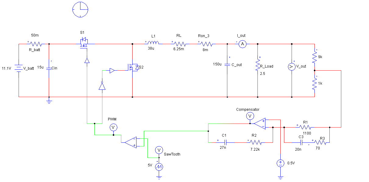
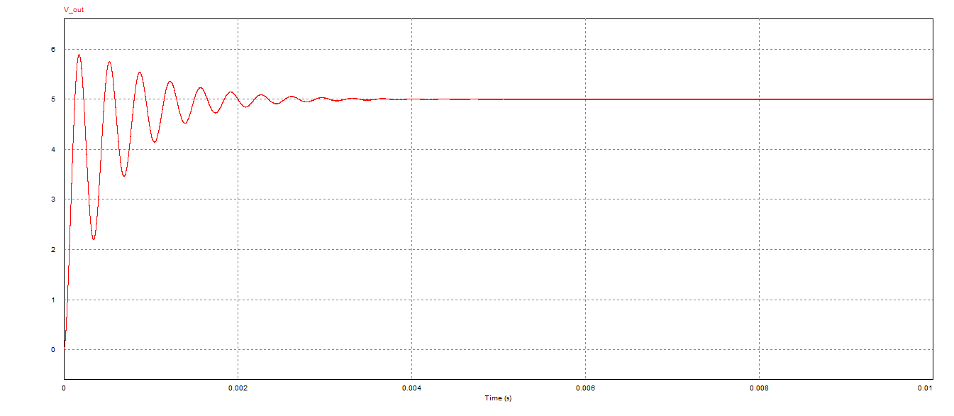
I am having trouble in tuning the PID control loop of the synchronous Buck converter. Figure 1 shows the circuit and figure 2 shows the response. I want the output voltage at 5V without any ringing and settling time is not important for me, however I am unable to tune this damn controller circuit :)

Circuit.png

Figure 1.
Response.png

Figure 2.

Also attached is the PSIM 9 file for this circuit. I used the K factor method to design the controller but proper could not damp the resonances properly. Any help and any guidance will be highly appreciated.

Thank you.
 

Attachments

  • Boost_Forward_CL_Compensated.rar
    8.1 KB · Views: 209

Hi,

the feedback voltage divider results in a 900 Ohms source impedance.
I guess R3 with 70 Ohms is rather useless. And C3 can not act as a proper "D" part.

Basically for low frequencies the Error amplifier input impedance is 2k Ohms and for high frequencies about 900 Ohms.
Crossover at about 7200 Hz.

What happens if you just increase C1 to 100nF? (without detailed analysis)
But I think it´s better to connect the right side of C3 to the output.

***
Indeed the ringing is quite expectable because of the integrating part of your error amplifier.

Klaus
 

Klaus's tip's sound good.

Also, please tell what is Fsw?

Also, try the following to see what it does.....

C1 = 10n
R2=1k
R1=47K
C3=47n
R3=1K


....if still not right, then make C3=100n & R3 = 330R


..if still not right, then add 100n across the 9k upper divider resistor

..if still not right, then make C1=4n7 and R2 = 4k7

I see you are in voltage mode, so you use type 3.

Ill find the voltage mode power stage txfer function in the meantime.
Also, what is your modulator gain?
--- Updated ---

for v mode the modulator gain is some function of sawtooth delta, and control voltage max...ill look it up and get back...then we can make out the bodes.
 
Last edited:

Hi,

the feedback voltage divider results in a 900 Ohms source impedance.
I guess R3 with 70 Ohms is rather useless. And C3 can not act as a proper "D" part.

Basically for low frequencies the Error amplifier input impedance is 2k Ohms and for high frequencies about 900 Ohms.
Crossover at about 7200 Hz.

What happens if you just increase C1 to 100nF? (without detailed analysis)
But I think it´s better to connect the right side of C3 to the output.

***
Indeed the ringing is quite expectable because of the integrating part of your error amplifier.

Klaus
Thank you Klaus, indeed increasing the C3 to 100nF made the plot a little bit better, around 10ms, the 2nd order response is dominant, then the response turns into the first order type as seen in the figure. I tried to connect the C3 directly to the output but it didn't make much of a difference. You are right about the source impedance of 900 ohms, the problem is that R1 is parallel to R3+(1/sC3), so there are no series connected elements otherwise I would have used the source impedance as a part of the transfer function. Here is the resulting plot when I increased C1 to 100nF.
C3_100nF.png


At least it solved the overshoot problem but the ringing is still present unfortunately. I don't really like designing using the phase margin technique, it never seems to work properly.

Zahid.
 

Hi,

I´d say it doesn´t look bad. 90% within 3ms. No real overshot.

C1 is the integrating capacitor
C3 is the differential capacitor. It has limted function when connelcted like in post#2.

The ringing is typical for an integrating error amplifier (as long as not compensated for this).
Imagine: As long as Vout is not at it´s setpoint the integrator voltage increases. (ignoring the D part) And Vout eventually is at it´s setpoint, then the I part is at it´s maximum --> driving the output even higher. Overshot. And it "needs" the overshot to get the I part do decrease.

I´m interested in seeing
* the error amplifier output plot
* and the C1 voltage plot.

****

You may try to "limit" C1 voltage ... to limit the overshot

Currently your regulator should be in stable state:
* when both error amplifier inputs are 0.5V
* when duty cycle is about 45%
* when error amplifier output is at 2.25V
...and ideally then the C1 voltage is about 1.75V. (Please check this with your simulation)

You could improve the circuit in a way that C1 voltage becomes zero in ideal case.
This could be done by changing the triangle range 0V..1.11V.
Then you are able to limit the C1 voltage with antiparallel diodes.

Klaus
 

Klaus's tip's sound good.

Also, please tell what is Fsw?

Also, try the following to see what it does.....

C1 = 10n
R2=1k
R1=47K
C3=47n
R3=1K


....if still not right, then make C3=100n & R3 = 330R


..if still not right, then add 100n across the 9k upper divider resistor

..if still not right, then make C1=4n7 and R2 = 4k7

I see you are in voltage mode, so you use type 3.

Ill find the voltage mode power stage txfer function in the meantime.
Also, what is your modulator gain?
--- Updated ---

for v mode the modulator gain is some function of sawtooth delta, and control voltage max...ill look it up and get back...then we can make out the bodes.
Thanks a lot for your help, I forgot to write, the switching frequency is 100kHz, here are the outcomes for the values used. It seems that there are optimal values that are present but I am unable to tune them.

For
C1 = 10n, R2=1k, R1=47K, C3=47n, R3=1K, the system is unstable and oscillates as shown below.
reply_001.png


For
C1 = 10n, R2=1k, R1=47K, C3=100n, R3=330, Stable but oscillation is present as shown below.
reply_002.png


For
C1 = 10n, R2=1k, R1=47K, C3=100n, R3=330, and 100n in series with the 9k divider resistor, unexpected results.
reply_003.png


C1 = 4.7n, R2=4.7k, R1=47K, C3=100n, R3=330, pretty much accomplished, if we could just get rid of these pesky ringings, pretty much the job is done here :D
reply_004.png

Thank you a lot for your help :)

Zahid.
 

Hi,

I´d say it doesn´t look bad. 90% within 3ms. No real overshot.

C1 is the integrating capacitor
C3 is the differential capacitor. It has limted function when connelcted like in post#2.

The ringing is typical for an integrating error amplifier (as long as not compensated for this).
Imagine: As long as Vout is not at it´s setpoint the integrator voltage increases. (ignoring the D part) And Vout eventually is at it´s setpoint, then the I part is at it´s maximum --> driving the output even higher. Overshot. And it "needs" the overshot to get the I part do decrease.

I´m interested in seeing
* the error amplifier output plot
* and the C1 voltage plot.

****

You may try to "limit" C1 voltage ... to limit the overshot

Currently your regulator should be in stable state:
* when both error amplifier inputs are 0.5V
* when duty cycle is about 45%
* when error amplifier output is at 2.25V
...and ideally then the C1 voltage is about 1.75V. (Please check this with your simulation)

You could improve the circuit in a way that C1 voltage becomes zero in ideal case.
This could be done by changing the triangle range 0V..1.11V.
Then you are able to limit the C1 voltage with antiparallel diodes.

Klaus
Hello Kalus, at steady state, the error amplifier output and C1 output voltages are around 2.25 and 1.75 volts respectively. Here is the plot.
Probes.png


I will try to limit the voltages and post the result again. Thanks a lot for the feedback :)

Zahid.
 

the error amplifier output and C1 output voltages are around 2.25 and 1.75 volts respectively.
then my mind calculation wasn´t that bad..

According the plot of post#7 you could even more decrease the C1 value.

Klaus

added:
regarding the "unexpected" behaviour in post#6:
This is just a pure "D" behaviour .. means limited dV/dt.
 

Hi,

I´d say it doesn´t look bad. 90% within 3ms. No real overshot.

C1 is the integrating capacitor
C3 is the differential capacitor. It has limted function when connelcted like in post#2.

The ringing is typical for an integrating error amplifier (as long as not compensated for this).
Imagine: As long as Vout is not at it´s setpoint the integrator voltage increases. (ignoring the D part) And Vout eventually is at it´s setpoint, then the I part is at it´s maximum --> driving the output even higher. Overshot. And it "needs" the overshot to get the I part do decrease.

I´m interested in seeing
* the error amplifier output plot
* and the C1 voltage plot.

****

You may try to "limit" C1 voltage ... to limit the overshot

Currently your regulator should be in stable state:
* when both error amplifier inputs are 0.5V
* when duty cycle is about 45%
* when error amplifier output is at 2.25V
...and ideally then the C1 voltage is about 1.75V. (Please check this with your simulation)

You could improve the circuit in a way that C1 voltage becomes zero in ideal case.
This could be done by changing the triangle range 0V..1.11V.
Then you are able to limit the C1 voltage with antiparallel diodes.

Klaus
You could improve the circuit in a way that C1 voltage becomes zero in ideal case.
This could be done by changing the triangle range 0V..1.11V.
Then you are able to limit the C1 voltage with antiparallel diodes.


I am using the saw-tooth as a modulator, and set its peak value to 5 Volts since I will use TL494 to design the circuit, and it has a reference voltage of 5 volts. I didn't understand the anti-parallel diodes concept, how do I place them(series or parallel or both) to make the C1 capacitor voltage go to 0V? Thanks a lot!

Zahid.
 

Hi,

for making C1 voltage zero, you need both sides equal.
Right side is 0.5V
so you need to make left side 0.5V, too. This can be done with a triangle 0V .. 1.1V.
(simple to do in simulation)

Alternative:
For sure you can make the right side of C1 = 2.25V .. but I guess this is more difficult.

Limiting C1 voltage:
"two antiparallel diodes across C1" says it all. Nothing in series.

Klaus
 

This was the best I could get with the current type-II configuration, the rise time oscillations just won't fade away, apparently, the compensator complex pole attenuation is not high enough at the resonance frequency of the converter.
best2.png


This is the response.
best.png


By putting anti-parallel diodes across the capacitor C1, the capacitor voltage does not go to zero but stays at 0.8 volts.

Zahid.
 

Thanks Zahid, also, if you like, we can start with the almost good values at the bottom of your post #6..
C1 = 4.7n, R2=4.7k, R1=47K, C3=100n, R3=330

...from here, adjust as follows...
Put just 10n across the 9k upper divider resistor....also...
Reduce R3 from 330R to try and damp out the ringings at start-up-rise

...Then increase R1 to 82k and go again from 330R downwards, still with 10n across the upper 9k.

Increasing R1 reduces the gain, and having C3 and R3 across R1 helps to prevent messigng the phase up when the gain is reduced.

Calculate the ringing frequency.....is it equal to the resonance frequency of Lout & Cout?
....If so it means your crossover freq is too close to this resonance, and as such, there is no way you will avoid ringing until you get x'over away from f(res).
[EDIT....sorry i just saw you are aware of this]

....i believe you could also solve the problem by using current mode control.....CMC takes out one of the poles at the output.....and stops it looking like an LC filter.

By the way, what ESR do you have in Cout?....no ESR will make it ring easily.
....
 
Last edited:

Thanks Zahid, if we start with the almost good values at the bottom of your post #6..
C1 = 4.7n, R2=4.7k, R1=47K, C3=100n, R3=330

...from here, adjust as follows...
Put just 10n across the 9k upper divider resistor....also...
Reduce R3 from 330R to try and damp out the ringings at start-up-rise

...Then increase R1 to 82k and go again from 330R downwards, still with 10n across the upper 9k.

Increasing R1 reduces the gain, and having C3 and R3 across R1 helps to prevent messigng the phase up when the gain is reduced.

Calculate the ringing frequency.....is it equal to the resonance frequency of Lout & Cout?
....If so it means your crossover freq is too close to this resonance, and as such, there is no way you will avoid ringing until you get x'over away from f(res).
[EDIT....sorry i just saw you are aware of this]

....i believe you could also solve the problem by using current mode control.....CMC takes out one of the poles at the output.....and stops it looking like an LC filter.

By the way, what ESR do you have in Cout?....no ESR will make it ring easily.
....
I didn't account for the ESR of the output capacitor and the inductance model is also non-saturating, this is a first order design of the converter and probably I will have to redesign the compensator, but I finally understood the concept of the effect of the gain on the poles and zeroes of the PID compensator. I will post an update with all the necessary updates, thanks @cupoftea and @KlausST for your help :)
 

Hi,
By putting anti-parallel diodes across the capacitor C1, the capacitor voltage does not go to zero but stays at 0.8 volts.
Sure.
Read what I´ve written.
--> You can zero the voltage C1 with adjusting the triangle amplitude.

After that you can limit the C1 voltage with the anti parallel diodes. (limit to about +/- 0.6V)

Klaus
 

Hi,

Sure.
Read what I´ve written.
--> You can zero the voltage C1 with adjusting the triangle amplitude.

After that you can limit the C1 voltage with the anti parallel diodes. (limit to about +/- 0.6V)

Klaus
I don't want to bother you too much (insert sweaty smiley emoji here :D) but, I don't know

Limiting C1 voltage:
"two antiparallel diodes across C1" says it all.

what this means. Like this? I attached a photo.


antiparallel.png
 

Hi,

correct.
But now I see you modified R2, thus you don´t have almost no P part anymore. Then you limit the total output range.

Klaus
 

For
C1 = 10n, R2=1k, R1=47K, C3=100n, R3=330, and 100n in series with the 9k divider resistor, unexpected results.
...OK thanks, but the 100n was supposed to be in pllel with the 9k, not in series
 

Solution
Voltage mode control has to be slow and damped,

for max phase lift , R1 = 100k, R2 = 10k

then, C1 = 15nF ( 100Hz ),

for the speed up, R3 = 22k, C3 = 22n


you're welcome ....
 

Hello all,

After redesigning the closed loop control, was finally able to get the required overshoot of 0.2 volts. Here is the circuit and the output voltage response respectively.
Buck_Forward.png

Vout.png


Since most IC's have built in soft-start function, the overshoot will be lower than 5.2 volts,( I hope). Thanks to all you guys for the amazing help.
--- Updated ---

...OK thanks, but the 100n was supposed to be in pllel with the 9k, not in series
You are right, 100n was supposed to be in parallel with 9k, i messed up there.
 

Status
Not open for further replies.

Similar threads

Part and Inventory Search

Welcome to EDABoard.com

Sponsor

Back
Top