Continue to Site

Welcome to EDAboard.com

Welcome to our site! EDAboard.com is an international Electronics Discussion Forum focused on EDA software, circuits, schematics, books, theory, papers, asic, pld, 8051, DSP, Network, RF, Analog Design, PCB, Service Manuals... and a whole lot more! To participate you need to register. Registration is free. Click here to register now.

Time step error due to connection between DC supply and IC large-signal model - ADS

Status
Not open for further replies.

mohamis288

Full Member level 3
Joined
Mar 1, 2022
Messages
164
Helped
0
Reputation
0
Reaction score
1
Trophy points
18
Activity points
1,235
Hello,

I am doing transient simulation on a circuit including a NXP IC large-signal model. I faced with a Time step error. after checking all the connection in my circuit, I realized that the problem occurred at the connection between DC supply and IC large-signal model. The picture this part of circuit is in the following:
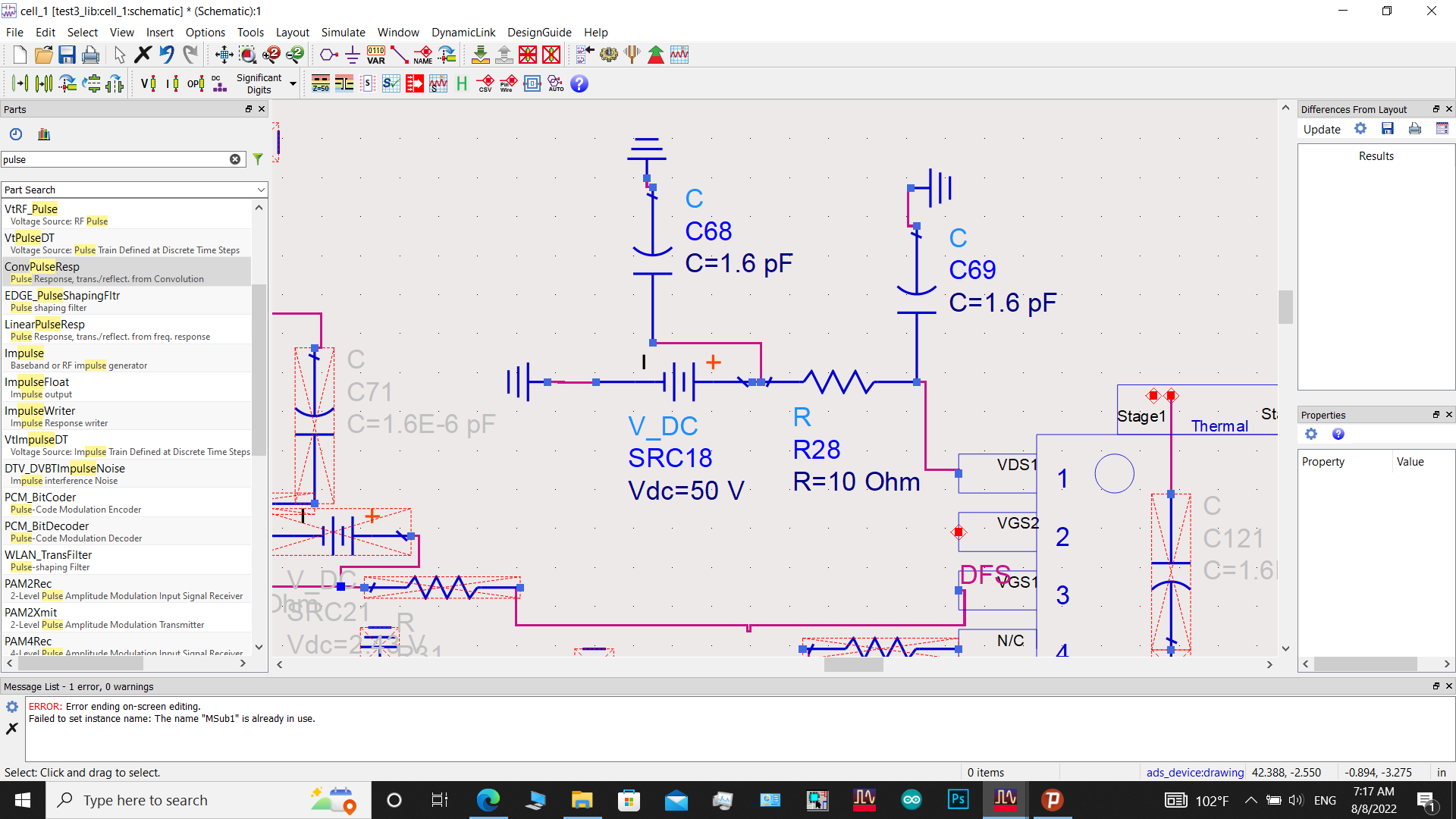
Screenshot (268).png


"VDS1" is the mentioned node. Whatever I change the parameters in my simulation ( changing the capacitors value, resistor value, transient simulation parameters and etc), nothing will change. I do not have any problem with other DC connections, for instance, "VGS2", "VGS1", "VDS2". Do you have any solution for this?
 

If you are allowed to peer into the "large signal model",
do so. You may find a nest of ideal sources and maybe
even behavioral code, which tends to be where numerical
problems breed (especially conplex controlled sources
without "limit" features, can blow up small errors, or create
error residues which never go away enough to satisfy
convergence.

You could perhaps (if model is not encrypted) excise the
portion attached to "VDS1" and fellow travelers, and try
aplying the same simulation conditions to a smaller "debug
surface".

Might look at that 50V supply and make sure it's within
the range that the "large signal model" purports to work.
Might the supply setting be violating the "fit-range" of the
model and blowing up as a result?

What happens if you ramp the V_DC supply after the
other supplies are stable? Perhaps some behavior will
yield clues, if you try.
 

    mohamis288

    Points: 2
    Helpful Answer Positive Rating
If you are allowed to peer into the "large signal model",
do so. You may find a nest of ideal sources and maybe
even behavioral code, which tends to be where numerical
problems breed (especially conplex controlled sources
without "limit" features, can blow up small errors, or create
error residues which never go away enough to satisfy
convergence.

You could perhaps (if model is not encrypted) excise the
portion attached to "VDS1" and fellow travelers, and try
aplying the same simulation conditions to a smaller "debug
surface".

Might look at that 50V supply and make sure it's within
the range that the "large signal model" purports to work.
Might the supply setting be violating the "fit-range" of the
model and blowing up as a result?

What happens if you ramp the V_DC supply after the
other supplies are stable? Perhaps some behavior will
yield clues, if you try.
Hello,
Thank you for your answer. I tried it out right now. If I decrease the value of V_DC from 50 volts down to 5 volts, the problem will be solved. But, as per the datasheet, we are free to choose VDS1 in the range ((0< ... <100 volts )), which the typical value is fixed at 50 volts.
Moreover, if use a "ramp()" function as the DC voltage for V_DC component, the problem will be solved. But, I want a fixed signal after a ramp, so this choice is not going to helpful. Alternatively, I use the recommendation in the following link, where I faced the same error even by using different values for the "pwl()" function:

https://www.edaboard.com/threads/how-to-generate-a-ramp-voltage-supply-in-ads.403734/#post-1739203

This is more than two weeks spending on this tedious problem.
 

Status
Not open for further replies.

Part and Inventory Search

Welcome to EDABoard.com

Sponsor

Back
Top