dirac16
Member level 5
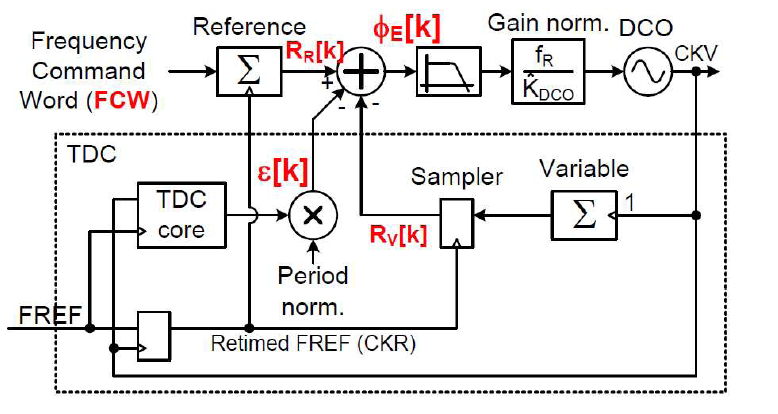
I have designed a time to digital converter (TDC) suitable for all-digital PLL (ADPLL) applications. As I don't have opportunity to validate the proposed TDC in a real chip, I tried to follow the approach proposed here (ieeexplore.ieee.org/document/4476201) to simulate ADPLL's behavior in the time domain using a high-level programming language such as Matlab. The following picture depicts ADPLL block diagram in phase domain. This picture is for your reference so you can refer to it when you need.

The following pseudo code is just an example of a type-I PLL that integrates my_TDC as the block responsible for fractional phase error measurement. A call to my_TDC(Tin) gives the output code relevant to the input time Tin. The output code is actually converted to decimal so that it can be useful.
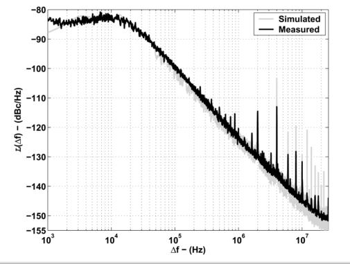
The above pseudo code doesn't do anything useful yet. Since TDC is notorious for in-band phase noise degradation, I need to find out the output phase noise by some sort of post processing on the variable time stamps, tV. The thing I think of is find phase noise due to period deviation, TDEV. The relation between TDEV and phase noise is straightforward: Phase_noise = 2pi * TDEV/TV. The thing now is I don't know (1) where to add this equation in the code above, and (2) how to take PSD of the resulted phase noise. These two things are really what I am stuck at. The figure below is one example of the kind of plot I need to generate. The figure measures phase noise with respect to offset frequency.

The following pseudo code is just an example of a type-I PLL that integrates my_TDC as the block responsible for fractional phase error measurement. A call to my_TDC(Tin) gives the output code relevant to the input time Tin. The output code is actually converted to decimal so that it can be useful.
Code:
// Parameter definitions
def Fo = 2.44e9             // Free running DCO frequency
def TV = 1/Fo
def FR = 26e6               // Reference frequency
def TR = 1/FR
def Fdes = 2e9              // Desired DCO frequency
def FCW = Fdes/FREF         // Frequency command word

for every FR

    RR = RR + FCW           // Reference phase accumulation; RR initially
                            // set to 0
    tR = tR + TR            // Reference time stamps; tR initially set to 0

    while tV < tR
        RV = RV + 1         // Variable phase accumulation; RV initially set
                            // to 0
        tV = tV + TV + TDEV // Variable time stamps; tV initially set to 0

    end

    dtr = tR - tV           // Time difference between first rising edge of
                            // FR and DCO clocks

    e = my_TDC(dtr)         // Fractional phase error converted to digital
                            // by my_TDC

    PHE = RR - (RV + e)     // Phase error

    NTW = a*PHE             // Normalized tuning word: Type-I PLL
    FDEV = NTW*FR           // Frequency deviation
    TDEV = - FDEV/Fo^2      // Frequency deviation converted to period
                            // deviation

end
The above pseudo code doesn't do anything useful yet. Since TDC is notorious for in-band phase noise degradation, I need to find out the output phase noise by some sort of post processing on the variable time stamps, tV. The thing I think of is find phase noise due to period deviation, TDEV. The relation between TDEV and phase noise is straightforward: Phase_noise = 2pi * TDEV/TV. The thing now is I don't know (1) where to add this equation in the code above, and (2) how to take PSD of the resulted phase noise. These two things are really what I am stuck at. The figure below is one example of the kind of plot I need to generate. The figure measures phase noise with respect to offset frequency.