Continue to Site

Welcome to EDAboard.com

Welcome to our site! EDAboard.com is an international Electronics Discussion Forum focused on EDA software, circuits, schematics, books, theory, papers, asic, pld, 8051, DSP, Network, RF, Analog Design, PCB, Service Manuals... and a whole lot more! To participate you need to register. Registration is free. Click here to register now.

this circuit FAILED on SS corner. I don't know why

Status
Not open for further replies.

allennlowaton

Full Member level 5
Joined
Oct 5, 2009
Messages
247
Helped
3
Reputation
6
Reaction score
3
Trophy points
1,298
Location
Taiwan
Activity points
3,066
Hello EDA felows,

I had made a corner simulation of this circuit and I found out that it failed on the SS corner.
I can't explain why.
Do I need a start-up circuit for this?

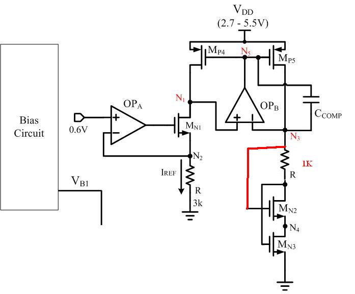
Below is the circuit diagram.


Below also are the pertinent node voltages.


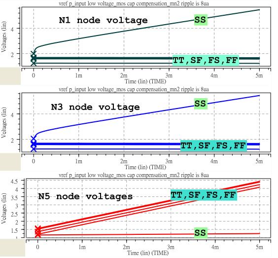
The DC output voltages of OPA in all corners are the same.

Regards,
 

Pls also show voltage for N2

---------- Post added at 02:29 ---------- Previous post was at 02:26 ----------

and VB1 for all corners.
 
the voltages at n2 on all corners are constant at 0.6V...

---------- Post added at 02:35 ---------- Previous post was at 02:30 ----------

the voltages at VB1:
TT - 788mV
SS - 900mV
SF - 1V
FS - 1V
FF - 800mV
 

I guess in SS corner VT for NMOS is too high. And Mn2 also have body effect that will increase VT further.
 
I did a simulation using an ideal OP for the OPB and it works well on all corners.
Now, I don't know where to start the debugging.
 

thank you and hello leo...
this is the resulting graph of your suggestion.(N1 and N3 node voltages are shown)


N1 and N3 should be a constant value, not a ramp.
 

thanks leo_o2..you're right..the problem is with VB1.
I increased it a bit and the circuit is now working perfectly on all corners.
 

If my schematic doesn't work well, you should have a big increase for W/L of Mn2 and Mn3.
thank you and hello leo...
this is the resulting graph of your suggestion.(N1 and N3 node voltages are shown)


N1 and N3 should be a constant value, not a ramp.
 
I just used the VB2 from the bias (VB2>VB1).In fact, I decreased the size of Mn2 (by 10 times) so that most the drop of Mn2 is much more higher than that of the Mn3. As much as possible I want a very low voltage of MN3 which also happens to be the node voltage of N4.

From this experimentation, I found out that the + terminal of the OP copied from the - terminal. I always believe before, that - terminal is the one who do copying.
 

Understand your requirement now. It will be OK.

---------- Post added at 03:09 ---------- Previous post was at 02:49 ----------

Another way for your requirement:
 
Understand your requirement now. It will be OK.

---------- Post added at 03:09 ---------- Previous post was at 02:49 ----------

Another way for your requirement:

so nice of you leo_o2...thank you very much...
 

Status
Not open for further replies.

Part and Inventory Search

Welcome to EDABoard.com

Sponsor

Back
Top