Kgonz
Newbie level 5
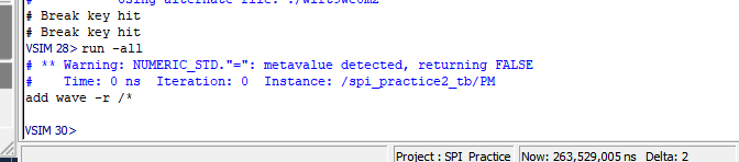
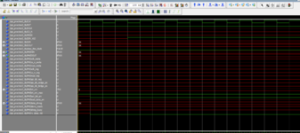
Hello, i am trying to learn how to implement an SPI Slave for work. this is the my first time writing any module so i decided to try to build a test bench around someones slave module i found online. i wrote the test bench but when i go to simulation i get a bunch of signals showing U and im not sure why i also receive a warning coming from the test bench. im not really sure what the problem is any help is appreciated Ive attached all relevant information below.
SPI SLAVE
SPI SLAVE
- --------------------------------------------------------------------------------
- -- PROJECT: SPI SLAVE FOR FPGA
- --------------------------------------------------------------------------------
- -- AUTHORS: Jakub Cabal <jakubcabal@gmail.com>
- -- LICENSE: The MIT License, please read LICENSE file
- -- WEBSITE: https://github.com/jakubcabal/spi-fpga
- --------------------------------------------------------------------------------
- library IEEE;
- use IEEE.STD_LOGIC_1164.ALL;
- use IEEE.NUMERIC_STD.ALL;
- use IEEE.MATH_REAL.ALL;
- -- THE SPI SLAVE MODULE SUPPORT ONLY SPI MODE 0 (CPOL=0, CPHA=0)!!!
- entity SPI_SLAVE1 is
- Generic (
- WORD_SIZE : natural := 8 -- size of transfer word in bits, must be power of two
- );
- Port (
- CLK : in std_logic; -- system clock
- RST : in std_logic; -- high active synchronous reset
- -- SPI SLAVE INTERFACE
- SCLK : in std_logic; -- SPI clock
- CS_N : in std_logic; -- SPI chip select, active in low
- MOSI : in std_logic; -- SPI serial data from master to slave
- MISO : out std_logic; -- SPI serial data from slave to master
- -- USER INTERFACE
- DIN : in std_logic_vector(WORD_SIZE-1 downto 0); -- data for transmission to SPI master
- DIN_VLD : in std_logic; -- when DIN_VLD = 1, data for transmission are valid
- DIN_RDY : out std_logic; -- when DIN_RDY = 1, SPI slave is ready to accept valid data for transmission
- DOUT : out std_logic_vector(WORD_SIZE-1 downto 0); -- received data from SPI master
- DOUT_VLD : out std_logic -- when DOUT_VLD = 1, received data are valid
- );
- end entity;
- architecture RTL of SPI_SLAVE1 is
- constant BIT_CNT_WIDTH : natural := natural(ceil(log2(real(WORD_SIZE))));
- signal sclk_meta : std_logic;
- signal cs_n_meta : std_logic;
- signal mosi_meta : std_logic;
- signal sclk_reg : std_logic;
- signal cs_n_reg : std_logic;
- signal mosi_reg : std_logic;
- signal spi_clk_reg : std_logic;
- signal spi_clk_redge_en : std_logic;
- signal spi_clk_fedge_en : std_logic;
- signal bit_cnt : unsigned(BIT_CNT_WIDTH-1 downto 0);
- signal bit_cnt_max : std_logic;
- signal last_bit_en : std_logic;
- signal load_data_en : std_logic;
- signal data_shreg : std_logic_vector(WORD_SIZE-1 downto 0);
- signal slave_ready : std_logic;
- signal shreg_busy : std_logic;
- signal rx_data_vld : std_logic;
- begin
- -- -------------------------------------------------------------------------
- -- INPUT SYNCHRONIZATION REGISTERS
- -- -------------------------------------------------------------------------
- -- Synchronization registers to eliminate possible metastability.
- sync_ffs_p : process (CLK)
- begin
- if (rising_edge(CLK)) then
- sclk_meta <= SCLK;
- cs_n_meta <= CS_N;
- mosi_meta <= MOSI;
- sclk_reg <= sclk_meta;
- cs_n_reg <= cs_n_meta;
- mosi_reg <= mosi_meta;
- end if;
- end process;
- -- -------------------------------------------------------------------------
- -- SPI CLOCK REGISTER
- -- -------------------------------------------------------------------------
- -- The SPI clock register is necessary for clock edge detection.
- spi_clk_reg_p : process (CLK)
- begin
- if (rising_edge(CLK)) then
- if (RST = '1') then
- spi_clk_reg <= '0';
- else
- spi_clk_reg <= sclk_reg;
- end if;
- end if;
- end process;
- -- -------------------------------------------------------------------------
- -- SPI CLOCK EDGES FLAGS
- -- -------------------------------------------------------------------------
- -- Falling edge is detect when sclk_reg=0 and spi_clk_reg=1.
- spi_clk_fedge_en <= not sclk_reg and spi_clk_reg;
- -- Rising edge is detect when sclk_reg=1 and spi_clk_reg=0.
- spi_clk_redge_en <= sclk_reg and not spi_clk_reg;
- -- -------------------------------------------------------------------------
- -- RECEIVED BITS COUNTER
- -- -------------------------------------------------------------------------
- -- The counter counts received bits from the master. Counter is enabled when
- -- falling edge of SPI clock is detected and not asserted cs_n_reg.
- bit_cnt_p : process (CLK)
- begin
- if (rising_edge(CLK)) then
- if (RST = '1') then
- bit_cnt <= (others => '0');
- elsif (spi_clk_fedge_en = '1' and cs_n_reg = '0') then
- if (bit_cnt_max = '1') then
- bit_cnt <= (others => '0');
- else
- bit_cnt <= bit_cnt + 1;
- end if;
- end if;
- end if;
- end process;
- -- The flag of maximal value of the bit counter.
- bit_cnt_max <= '1' when (bit_cnt = WORD_SIZE-1) else '0';
- -- -------------------------------------------------------------------------
- -- LAST BIT FLAG REGISTER
- -- -------------------------------------------------------------------------
- -- The flag of last bit of received byte is only registered the flag of
- -- maximal value of the bit counter.
- last_bit_en_p : process (CLK)
- begin
- if (rising_edge(CLK)) then
- if (RST = '1') then
- last_bit_en <= '0';
- else
- last_bit_en <= bit_cnt_max;
- end if;
- end if;
- end process;
- -- -------------------------------------------------------------------------
- -- RECEIVED DATA VALID FLAG
- -- -------------------------------------------------------------------------
- -- Received data from master are valid when falling edge of SPI clock is
- -- detected and the last bit of received byte is detected.
- rx_data_vld <= spi_clk_fedge_en and last_bit_en;
- -- -------------------------------------------------------------------------
- -- SHIFT REGISTER BUSY FLAG REGISTER
- -- -------------------------------------------------------------------------
- -- Data shift register is busy until it sends all input data to SPI master.
- shreg_busy_p : process (CLK)
- begin
- if (rising_edge(CLK)) then
- if (RST = '1') then
- shreg_busy <= '0';
- else
- if (DIN_VLD = '1' and (cs_n_reg = '1' or rx_data_vld = '1')) then
- shreg_busy <= '1';
- elsif (rx_data_vld = '1') then
- shreg_busy <= '0';
- else
- shreg_busy <= shreg_busy;
- end if;
- end if;
- end if;
- end process;
- -- The SPI slave is ready for accept new input data when cs_n_reg is assert and
- -- shift register not busy or when received data are valid.
- slave_ready <= (cs_n_reg and not shreg_busy) or rx_data_vld;
- -- The new input data is loaded into the shift register when the SPI slave
- -- is ready and input data are valid.
- load_data_en <= slave_ready and DIN_VLD;
- -- -------------------------------------------------------------------------
- -- DATA SHIFT REGISTER
- -- -------------------------------------------------------------------------
- -- The shift register holds data for sending to master, capture and store
- -- incoming data from master.
- data_shreg_p : process (CLK)
- begin
- if (rising_edge(CLK)) then
- if (load_data_en = '1') then
- data_shreg <= DIN;
- elsif (spi_clk_redge_en = '1' and cs_n_reg = '0') then
- data_shreg <= data_shreg(WORD_SIZE-2 downto 0) & mosi_reg;
- end if;
- end if;
- end process;
- -- -------------------------------------------------------------------------
- -- MISO REGISTER
- -- -------------------------------------------------------------------------
- -- The output MISO register ensures that the bits are transmit to the master
- -- when is not assert cs_n_reg and falling edge of SPI clock is detected.
- miso_p : process (CLK)
- begin
- if (rising_edge(CLK)) then
- if (load_data_en = '1') then
- MISO <= DIN(WORD_SIZE-1);
- elsif (spi_clk_fedge_en = '1' and cs_n_reg = '0') then
- MISO <= data_shreg(WORD_SIZE-1);
- end if;
- end if;
- end process;
- -- -------------------------------------------------------------------------
- -- ASSIGNING OUTPUT SIGNALS
- -- -------------------------------------------------------------------------
- DIN_RDY <= slave_ready;
- DOUT <= data_shreg;
- DOUT_VLD <= rx_data_vld;
- end architecture;
- library IEEE;
- use IEEE.std_logic_1164.all;
- use IEEE.numeric_std.all;
- use IEEE.MATH_REAL.ALL;
- entity Spi_practice2_tb is
- end Spi_practice2_tb;
- architecture bench of Spi_practice2_tb is
- constant WORD_SIZE : integer := 8;
- constant clock_period: time := 10 ns;
- constant BIT_CNT_WIDTH : natural:= natural(ceil(log2(real(WORD_SIZE))));
- component SPI_SLAVE1
- port(
- CLK,RST,SCLK,CS_N,MOSI,DIN_VLD: in std_logic;
- MISO,DIN_RDY,DOUT_VLD: out std_logic;
- DIN: in std_logic_vector(WORD_SIZE-1 downto 0);
- DOUT: out std_logic_vector(WORD_SIZE-1 downto 0)
- );
- end component;
- signal CLK,RST,SCLK,CS_N,MOSI,DIN_VLD: std_logic;
- signal MISO,DIN_RDY,DOUT_VLD: std_logic;
- signal DIN: std_logic_vector(WORD_SIZE-1 downto 0);
- signal DOUT: std_logic_vector(WORD_SIZE-1 downto 0);
- signal stop_the_clock:boolean;
- signal sclk_meta : std_logic;
- signal cs_n_meta : std_logic;
- signal mosi_meta : std_logic;
- signal sclk_reg : std_logic;
- signal cs_n_reg : std_logic;
- signal mosi_reg : std_logic;
- signal spi_clk_reg : std_logic;
- signal spi_clk_redge_en : std_logic;
- signal spi_clk_fedge_en : std_logic;
- signal bit_cnt : unsigned(BIT_CNT_WIDTH-1 downto 0);
- signal bit_cnt_max : std_logic;
- signal last_bit_en : std_logic;
- signal load_data_en : std_logic;
- signal data_shreg : std_logic_vector(WORD_SIZE-1 downto 0);
- signal slave_ready : std_logic;
- signal shreg_busy : std_logic;
- signal rx_data_vld : std_logic;
- begin
- PM: entity work.SPI_SLAVE1
- port map (CLK => CLK,
- RST => RST,
- SCLK => SCLK,
- CS_N => CS_N,
- MOSI => MOSI,
- DIN => DIN,
- DIN_VLD => DIN_VLD,
- MISO => MISO,
- DIN_RDY => DIN_RDY,
- DOUT => DOUT,
- DOUT_VLD => DOUT_VLD);
- process
- begin
- RST <= '1';
- RST <= '0';
- wait for clock_period;
- spi_clk_fedge_en <= '1';
- cs_n_reg <= '0';
- wait for clock_period;
- DIN_VLD <= '1';
- cs_n_reg <= '1';
- rx_data_vld <= '1';
- wait;
- end process;
- process -- clock generation
- begin
- while not stop_the_clock loop
- CLK <= '0';
- wait for clock_period / 2;
- CLK <= '1';
- wait for clock_period / 2;
- end loop;
- wait;
- end process;
- end;