Continue to Site

Welcome to EDAboard.com

Welcome to our site! EDAboard.com is an international Electronics Discussion Forum focused on EDA software, circuits, schematics, books, theory, papers, asic, pld, 8051, DSP, Network, RF, Analog Design, PCB, Service Manuals... and a whole lot more! To participate you need to register. Registration is free. Click here to register now.

Symmetric non overlapping clock generator

Status
Not open for further replies.

mordak

Member level 5
Joined
Mar 8, 2013
Messages
82
Helped
0
Reputation
0
Reaction score
0
Trophy points
1,286
Location
Neverland
Activity points
2,134
Hi,

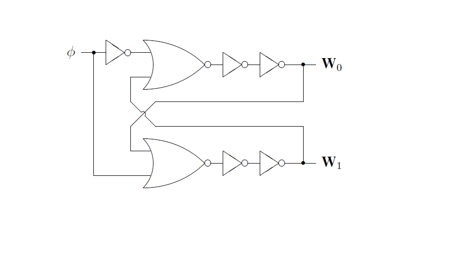
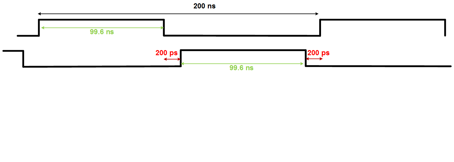
Implementing a non overlapping clock generator (NOCG) is fairly straightforward. But my problem is that the generated non-overlapped clocks are not symmetric (On time of the two non-overlapped clocks is slightly different). I read somewhere that adding an asymmetric transmission gate will help having symmetric clocks, but I could not get it work. I wonder if there is any NOCG circuit that gives symmetric output clocks.

Tnx
 

Since P types have higher RdsOn than N types for the same size, selective matching of turn on and off using a diode shunted gate resistors helps in tuning the symmetry.

Show your requirements by values and results with required load impedance and voltage range.

There is a wide range of applications for this and your question is vague.
Thanks for your comment! I use a NOCG like the one attached. The input clock is 100 MHz and W0 and W1 are connected to bunch of inverters. So I would say W0 and W1 would see a load of like 100 fF (both non overlapping clocks have an equal load to drive).


I noticed that there is 500 ps time difference between pulse widths of W0 and W1 (since these two clocks pass through asymmetric paths). Even 500 ps difference causes some distrotion in my circuit. So I want to make W0 and W1 completely symmetric (at least in simulation, though I know process variation will change that). I design the circuit in a 0.18 CMOS technology. BTW, I haven't heard of the diode shunted gate resistors, what is it? Is it suitable for an integrated circuit?

Tnx
 

Show your exact specs for symmetry error %, dead time, for dual clock outputs, the examine your prop. delay for each gate with tolerances. I normally worked with worst case tolerances over temp range in logic families, while you are designing by simulation but without specs on discrete gates.

R//CR gate drive is common in high power MOS where faster turn-off is needed to control ~1us dead time in full bridges with CISS in nF.
 
  • Like
Reactions: mordak

    mordak

    Points: 2
    Helpful Answer Positive Rating
Quite a few ECL chips have simultaneous inverting and non inverting outputs available, with theoretically zero skew between the two outputs provided they are similarly loaded.

If you require exact 50% duty cycle, a flip flop clocked at twice the required frequency is the usual solution.

Still not exactly clear as to your requirement.
 
  • Like
Reactions: mordak

    mordak

    Points: 2
    Helpful Answer Positive Rating
Does this circuit help?

1.png
 

Does this circuit help?

View attachment 130199


No. It helps to define your goals & specs on each gate and overall targets.

As @warpspeed indicated ECL like all CML has inherent symmetry, controlled impedance and fastest rise times, all important key metrics for xx ps control of edges.

Your first schema is the classic version.
 

Show your exact specs for symmetry error %, dead time, for dual clock outputs, the examine your prop. delay for each gate with tolerances. I normally worked with worst case tolerances over temp range in logic families, while you are designing by simulation but without specs on discrete gates.

R//CR gate drive is common in high power MOS where faster turn-off is needed to control ~1us dead time in full bridges with CISS in nF.

Quite a few ECL chips have simultaneous inverting and non inverting outputs available, with theoretically zero skew between the two outputs provided they are similarly loaded.

If you require exact 50% duty cycle, a flip flop clocked at twice the required frequency is the usual solution.

Still not exactly clear as to your requirement.

No. It helps to define your goals & specs on each gate and overall targets.

As @warpspeed indicated ECL like all CML has inherent symmetry, controlled impedance and fastest rise times, all important key metrics for xx ps control of edges.

Your first schema is the classic version.
Tnx for all the comments. The attached is an example of what I want.

There are a couple of things I need to describe:

I need to have non-overlapping clocks and dead zone, or duty cycle do not matter that much to me. What I have noticed in my simulations was that any mismatch between pulse width of two non overlapping clocks will introduce distortion in my system. So if 99.6 ns in the figure becomes 99.58 ns for one clock and for the other one becomes 99.62 ns, then I see distortions.

I really do not care if that 99.6 ns pulse width becomes 99.4 ns, as long as both clocks have the same pulse width. rise time and fall time also are not important factors to me.
I am looking for a circuit I can implement in CMOS technology to give me the same pulse width for the both non overlapping clocks. I appreciate if anyone can give me a hint how to implement that.

Thanks
 

What kind of visual distortion?
Attached is the power spectrum of the system, it is a converter and as you can see there is a distortion at Fs - Fin, close to 47.5 MHz that is merely due to the asymmetric non overlapping clocks I mentioned before.


Status
Not open for further replies.

Similar threads

Part and Inventory Search

Welcome to EDABoard.com

Sponsor

Back
Top